Hi Expert,
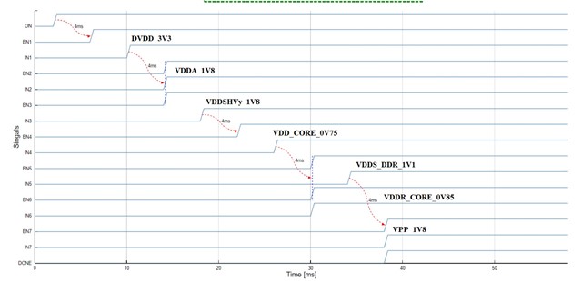
Please help to confirm whether the power sequence meets the spec requirements

Thanks
Daniel
This thread has been locked.
If you have a related question, please click the "Ask a related question" button in the top right corner. The newly created question will be automatically linked to this question.
Hi Expert,
Please help to confirm whether the power sequence meets the spec requirements

Thanks
Daniel
Hello Daniel,
Thank you for the query.
Could you pls describe the power solution used. Can you help me understand how the EN timing is controlled.
Please refer to the Power-up and power-down diagram in the datasheet.
Figure 7-5. Power-Up Sequencing
Figure 7-6. Power-Down Sequencing
Let me know if you have any questions.
Regards,
Sreenivasa
Hi Sreenivasa
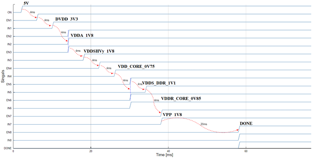
The complete Power-Up Sequencing is as follows.
Please help to confirm whether the power sequence meets the spec requirements

Is the Power-down sequence required only if VDDR_CORE is not greater than VDD_CORE +0.18V?
Doesn’t need to be considered when VDDR_CORE and VDD_CORE are the same 0.85V power source?

Thanks
Daniel
Hello Daniel,
Thank you.
Could you pls describe the power solution used. Can you help me understand how the EN timing is controlled if discrete supply is used.
Please refer to the Power-up and power-down diagram in the datasheet.
Figure 7-5. Power-Up Sequencing
Looks like the above diagram is in line with the datasheet diagram.
I cant see the MCU_PORZ and the SOC clock. I assume these signals are following the diagram.
Any reason for the 1.8V to be active during power-up. We would recommend this supply to be low during power up and enabled only when the eFuse is required to be programmed.
Power-down
The note above is for the core voltage. It is required to still follow the power-down sequence as per the diagram reference below.
Figure 7-6. Power-Down Sequencing
Regards,
Sreenivasa
Hello Daniel,
I am closing the thread since i have not heard from you.
Regards,
Sreenivasa