This thread has been locked.

If you have a related question, please click the "Ask a related question" button in the top right corner. The newly created question will be automatically linked to this question.

AM625: LPDDR4 spacing requirements

Part Number: AM625

Hi

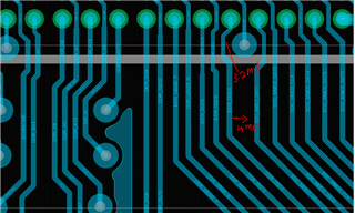
We would like to know regarding lpddr4 spacing requirements.As per TI recommendation its 4W except for certain cases where  its 3W. However in AM62xx or AM64xx evaluation board only 3W spacing is followed for all signal spacing.Nowhere 4W is followed. Please let us know if 3W spacing is sufficient.
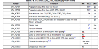
  • Yes, there is a note that says it can fall to 2w around the endpoints.  If you can only space them 3w in the middle, you should simulate your board to ensure no crosstalk and optimal signal integrity.

    Regards,

    James

  • ok.Another query is : How the impedance deviation is handled especially near the BGA fan out region by different trace width variation in AM62xx eval board.Near BGA its 3.2mil(which is as per the 0.5mm bga pitch)and then there is a change to 4 mi.l but stackup recommends 9.05mils. Why impedance is not matched for lpddr4 traces on the outer layers? Although 9.02 mils has to be followed as per stackup, only 4mils is followed in eval board.Pls clarify this

  • Premalatha, where in the stackup are you seeing 9.05mils?  Can you give more details?  Is this somewhere in the EVM design or the DDR layout app note?

    Regards,

    James  

  • Hi James,

    This is from the Evaluation board layout(PROC114E3).

  • Hi Premalatha,

    The trace width necks down to 3.2 mil to sneak through the 0.5mm pitch pads on the AM62x device, then it widens slightly to 4 mil to escape the footprint while maintaining 2W separation from the nearest traces.
    As soon as possible, the traces VIA down to an inner signal layer where the 40 ohm stripline impedance is satisfied with a 9 mil trace width.

    There is an impedance mismatch from the package pin to the VIA, but it is for a short distance of 200mil or so. The narrow trace will raise the impedance above the 40 ohm target. We simulate the design to ensure eye diagram margins.

    Manufacturability of the 3.2mil trace on the outer layer is a concern, so it is must only be used to neck down through the device pads.

    Ideally you should escape 0.5mm pitch parts on an unplated layer to improve manufacturability with such fine trace widths. Plating requires over etching to achieve desired trace width after plating. A fine trace risks forming an open (or undesired impedance) if etched too far. In this case, we chose to escape the outer two rows of BGAs on the top layer to avoid HDI VIA structures (and their cost).

    Hope this clarifies,
    Mark