Part Number: DRA726
At present we will replace J6 ECO DRA726APL2ABCQ1 to J6 DRA745BLGABCQ1 normal board, the chip will not run, we see the information below it seems that J6 and J6 Eco are compatible design.It should be possible to switch on.
1 The current phenomenon is that the main chip has been loading the data of the SD card, can measure to the CLK, CMD, D0 signal line on SDIO all the time there is data.Isn't the process of loading only once?I measured normal J6 board SDIO only once during the loading process (whether the card is inserted or not).
2 We also tried to change the BOOT boot configuration to USB EMMC boot (SYSBOOT[5:0]=000000), after the modification the SD card SDIO signal will no longer have a waveform.EMMC data on CMD and D0 energy to data (CLK runs on the inner layer and cannot be quantified).However, there is still no print information.(The EMMC has the start-up data for the previous J6).
3 We also tested the DDR clock is wavy, other signals are high, should not go to DDR this step.
4 We found a difference between the WAKE UP source for J6 eco and J6, just as our previous J6 was using WAKE UP 1, I tried to change PMIC_INT to WAKE UP3, or both WAKE UP 0 and WAKE UP 3 to low level, the phenomenon is still.Is our question now not related to WAKE??
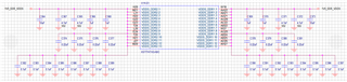
5 accessories for the current replacement of the J 6 motherboard schematic, please help analyze whether J6 and J6 ECO are different in hardware configuration, so now BOOT is not up, thank you ~