This thread has been locked.

If you have a related question, please click the "Ask a related question" button in the top right corner. The newly created question will be automatically linked to this question.

TDA4VE-Q1: SERDES0_REFCLK as an output clock

Part Number: TDA4VE-Q1

Hi,

is it possible to output 100MHz clock from SERDES0_REFCLK_P & SERDES0_REFCLK_N pins on TDA4VE (j721s2)?

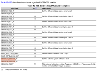
TDA4VE-Q1 datasheet (SPRSP62) lists SERDES0_REFCLK_PSERDES0_REFCLK_N as IO (input/output) pin type:

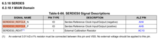
However, J721S2 TDA4VE TRM (SPRUJ08C) list those two pins as input only (not capable of clock output):


Could you clarify which one is correct?

And if clock output is possible, where to find details on how to do so?

BR,

Primoz

CC: 

  • For TDA4VE, need to use the PCIE_REFCLK output pins instead of SERDES_REFCLK. Below is an excerpt from the TRM that illustrates how to configure. Also note an errata on these pins (pasted below) that explains some of the confusion around REFCLK1 vs REFCLK3.

  • Hi ,

    first of all thank you for your reply and pointing out to attached documents.

    However I still have some questions:

    1) Can you say with 100% that SERDES0_REFCLK_P & SERDES0_REFCLK_N pins cannot be used as CLK outputs?

    2) If we output clock on pins PCIE_REFCLK1_P_OUT & PCIE_REFCLK1_N_OUT, do we need to supply reference clock on SERDES0_REFCLK_P & SERDES0_REFCLK_N pins? Or put differently, are SERDES0_REFCLK_P & SERDES0_REFCLK_N fully optional?

    3) I went through J721S2_Registers_230124.xlsx file (this is what we got from TI for j721s2 register map) and could not find any register for PCIE_REFCLK3_CLKSEL (I was only able to find register CTRL_MMR_PCIE_REFCLK1_CLKSEL -> PA: 0010 8074h). So I am not sure how to implement errata workaround.

    Thanks for your answers in advance,

    BR,

    Primoz

  • Hi ,

    I cannot enable clock output from PCIE_REFCLK1_P/N_OUT pins. Pins levels remain low all the time.

    Here is what I have tried so far:

    1) Enable PCIE_REFCLK1_P/N_OUT pins in (ACSPCIE0_CTRL → 0x00118090 register):

    devmem2 0x00118090 w 0x0

    → enable PAD0 IO buffers (clear bit 0)

    → enable PAD1 IO buffers (clear bit 1)

    → disable test mode (clear bit 8)

    STATUS:

    # devmem2 0x00118090

    /dev/mem opened.

    Memory mapped at address 0xffff82a57000.

    Read at address 0x00118090 (0xffff82a57090): 0x01000000

    Bandgap output OK!

    2) Select clock source by setting PCIE_REFCLK1_CLKSEL + PCIE_REFCLK3_CLKSEL (See errata i2308)

    devmem2 0x00108074 w 0x101

    devmem2 0x0010807C w 0x101

    → enable OUT_CLK_EN (set bit 8)

    → set mux to MAIN_PLL2_HSDIV4_CLKOUT (set bits 0-1 to 0x01)

    STATUS:

    # devmem2 0x00108074

    /dev/mem opened.

    Memory mapped at address 0xffffa839d000.

    Read at address 0x00108074 (0xffffa839d074): 0x00000000

    # devmem2 0x0010807C

    /dev/mem opened.

    Memory mapped at address 0xffffaec23000.

    Read at address 0x0010807C (0xffffaec2307c): 0x00000000

    NOTE: Values are not written correctly, read back is always 0x0!

  • I'm looping in another resource to help with programming instructions.

  • Hi ,

    I have finally managed to enable PCIE1_REFCLK. But I have to write PCIE_REFCLK1_CLKSEL + PCIE_REFCLK3_CLKSEL registers already in the bootloader. Writing in kernel or userspace has no effect.

    Do you have an idea why this is the case? e.g. Why some CTRL_MMR registers behave like that?