Hello,
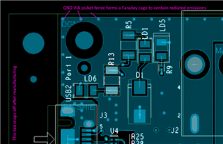
In the PCB layout file, I noticed that there is a copper pour ring around the entire board. It's connected to DGND and has vias along the edges, connecting to similar rings on the other layers.
What is the purpose of these? To protect traces carrying signals?
Below are screenshots of the board:
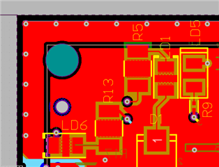
Close up: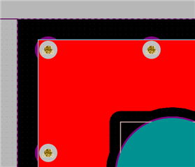
Thank you.