This thread has been locked.

If you have a related question, please click the "Ask a related question" button in the top right corner. The newly created question will be automatically linked to this question.

DDR3 Design Requirement for Keystone Devices

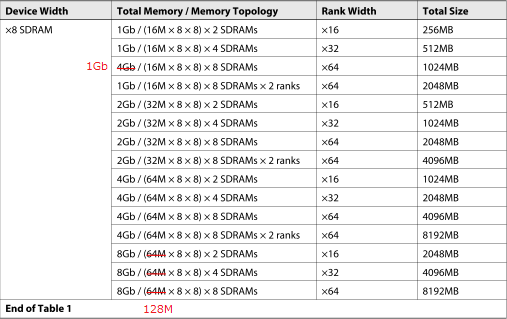
DDR3 Design Requirement for Keystone Devices p11 Table

I do not understand some part of the table.

Device Width Total Memory / Memory Topology Rank Width Total Size

x8 SDRAM 1Gb / (16M x 8 x 8) x 4 SDRAMS x32 512MB (2nd row of Table 1)

Column1 (Device width): This is the data width of the DDR3 SDRAM. Currently available are x8, x16, x32.

Column2 (Total Memory/Memory Topology): I do not understand this column. 

I understand that 16M (number of memory locations per bank) x 8 (device width) x 8 (number of banks) is the configuration for the DDR3 SDRAM.

But I do not understand the 1Gb. Initially I understand it to be 1Gb=16M*8*8 but 3rd row (4Gb / (16M x 8 x 8)) and other rows below proves otherwise. Could it be a typo?

I understand x2 SDRAMs to be the number of SDRAM for that topology. x8 SDRAMs x 2 Ranks => x 16 SDRAMs.

Column3 (Rank width): I do not understand this column.

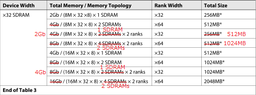
Rank width seems to be the device width * number of SDRAM. However, some rows (row 3, 4, 7, 8 in Table 3) again prove otherwise.

Column 4(Total size): I do not understand this column.

Total size seems to be memory size * number of RAM used. However, some row (row 3, 4, 7, 8 in Table 3) again prove otherwise.

I suspect there is a lot of typo in p11 and p12. Pls help to clarify to confirm my understanding. Thanks.

  • Wenjun,

    I reviewed Table 1, and there is one mistake on Line 3 - it should say 1Gb instead of 4Gb for the total memory.  Table 2 is correct, Table 3 needs to have some corrections made.  I'm not sure why but Lines 3,4,7 and 8 as listed are not only incorrect but in 7 & 8 are impossible to implement.

    Thanks for bringing this to our attention. We'll have it corrected in the next spin. 

    I'll try to clear up any confusion below.

    Total Memory = Total Memory of a single SDRAM Chip

    Total Size implemented = Total Memory * # SDRAM Chips used (This is irrespective of Rank Width of Device Width)

    2 Ranks means it has 2 sets of the listed SDRAM Chips connected up, but enabled on different CE's

    Rank Width is the width of Data Connected across a Rank (weather it's one or 2 ranks) we support x16, x32 and x64 - this does not impact the size calculation.

    Best Regards,

    Chad

  • Hi Chad,

    For Table1 and Table3, I understand it as follows.


    Is my understanding correct?

    Best regards,

    Daisuke


  • Daisuke,

    Yes, your corrections are accurate.  We will be updating this document in the next few months and will integrate these changes.

    Do you now understand the "Total Size" column?  This is the resulting addressible memory range in Bytes.

    Tom


  • Hi Tom,

    Thank you for your reply.

    Best regards,

    Daisuke