


Hello Engineer
I use VIN1A and VIN2A of TDA2SX to receive FPGA data, data bandwidth is 16bit,VIN interface uses falling edge sampling.
Testing found that CLK=50MHz data transmission is working normally, but data transmission errors occur when CLK=100MHz.
Other information as follows:
(1)in file sbl_utils_tda2xx_iodelay.c ,A _ DELAY、G_ DELAY of VIN1A and VIN2A has been modified to the data in the data manual as "VIP1-MANUAL2";
(2) The PCB bus lengths for VIN1A and VIN2A are as follows
unit:mil
| VIN1A | VIN2A | |
| FLD0 | 964.38 | 1208.46 |
| VSYNC0 | 1071.24 | 1296.38 |
| DE0 | 1089.33 | 1295.65 |
| CLK0 | 1177.78 | 1168.12 |
| D0 | 1075.47 | 1192.82 |
| D1 | 1066 | 1200.54 |
| D2 | 1007.05 | 1212.45 |
| D3 | 1010.52 | 1241.34 |
| D4 | 1032.85 | 1164.78 |
| D5 | 1060.14 | 1205.24 |
| D6 | 1033.93 | 1258.54 |
| D7 | 1020.63 | 1251.6 |
| D8 | 886.92 | 1204.3 |
| D9 | 881.83 | 1233.48 |
| D10 | 1133.07 | 1214.09 |
| D11 | 1143.78 | 1243.11 |
| D12 | 951.63 | 1264.25 |
| D13 | 942 | 1255.49 |
| D14 | 1077.85 | 1231.73 |
| D15 | 1070.27 | 1244.43 |
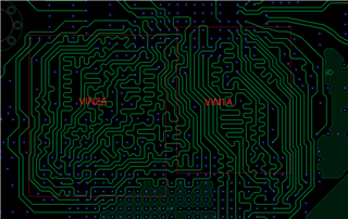
(3)The circuit layout of the PCB is as follows
Is it due to incorrect software delay time configuration or hardware error,Could you please provide some suggestions for debugging issues?
