This thread has been locked.

If you have a related question, please click the "Ask a related question" button in the top right corner. The newly created question will be automatically linked to this question.

DRA821U: DRA821U GPMC bus cycle in write access

Part Number: DRA821U
Other Parts Discussed in Thread: DRA821

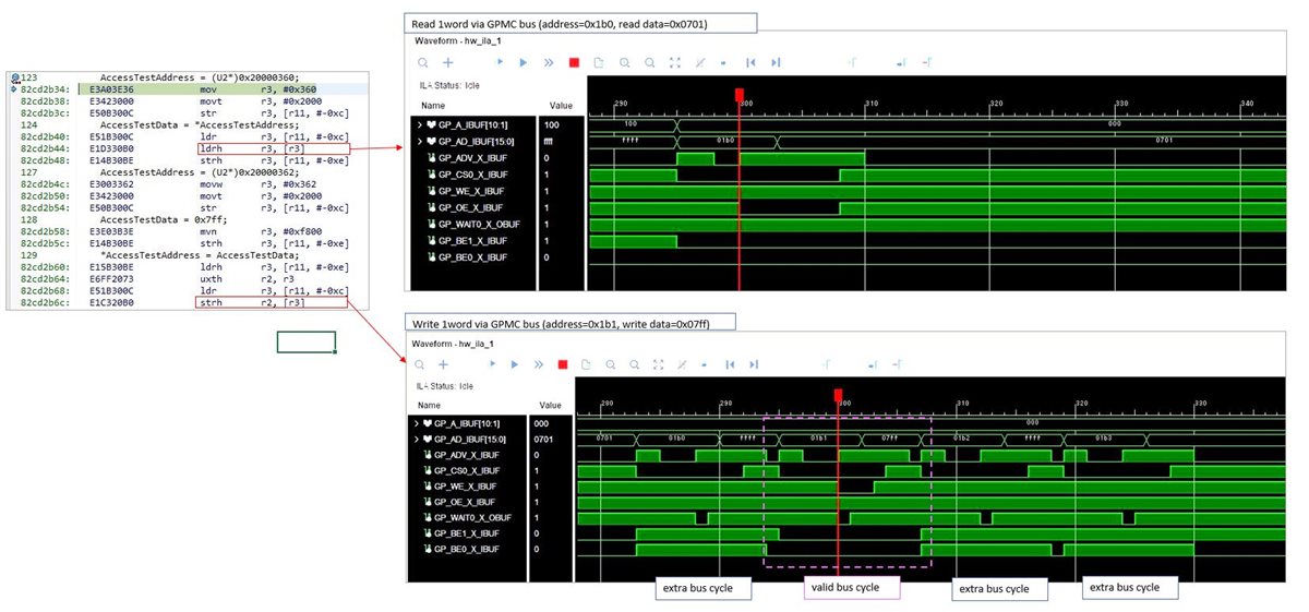
Our Prototype board uses GPMC Bus Interface to access target FPGA.
The target FPGA can be accessed normally via GPMC Bus, but in write operation, extra bus cycles are always observed in single word write access.
Is there some setting to suppress the generation of extra bus cycles ?

(1) GPMC Bus Cennection

DRA821U GPMC Port(Asynhronous, A/D-MUX mode, 16bit data size, use CS0-only, 128MB) <---> FPGA
interface signals: A[10:1],AD[15:0],CS0n,ADVn,WEn,OEn,BE1n,BE0n,WAIT0

(2) Observed interface signals

Waveforms of read/write access (from R-core)

regards,
Toshiya

  • Hello Toshiya-san,

    Can you summarize the basic modes of operation of the GPMC controller?  Can you reference which waveform in the TRM most closely matches your desired operating condition?

    Also, can you confirm the state of the WRITEMULTIPLE bit in the GPMC registers:

    Thanks

    Kyle

  • Hi, kcastille

    We referred to the following diagram and table.
    [Figure 12-2466. Asynchronous NOR Single Write Simplified Examples]
    [Table 12-6678. Asynchronous NOR Formulas Description]

    Here is the GPMC Bus WR/RD cycle of our design.

    And here is the GPMC register values of our current design.
    WRITEMULTIPLE parameter is set to '0'.

    Regards,
    Toshiya

  • Hello,

    From your initial figure I can see the code is doing LDRH and STRH from what appears to be a Cortex-R5 core.  The code looks like it could have an issue on the write side if a DSB is not used at the store.  If your MPU settings are for normal-non-cached or DEVICE, it is possible that write merging can happen.  This could result in a extra accesses on the writes, but it would not result in extra reads.  I would suggest you set this address region to 'StronglyOrdered" in the MPU and try the same code.   You could also experiment with the code and add DSBs after your writes to ensure the clear the boundary and are not merge candidates in a write buffer.   Sometimes people on purpose use DEVICE to get burst writes of element sizes to FIFOs.  As DEVICE attributes can preform much faster for a series of writes than StronglyOrdred, however, strange effects can happen if the properties are not understood.

    Regards,
    Richard W.
  • Hi, Richard

    Thank you for the advice.
    We tested several attribute setting for GPMC region.
    ATR_STRG, ATR_SDEV, ATR_NDEV shown below were tested, but we had same results. (read:1-cycle, write:4-cycle)

    /* Memory region attributes
    */
    #define ATR_STRG (0x00000000U) /* Strongly Ordered Strongly Ordered Shareable */
    #define ATR_SDEV (0x00000001U) /* Shared Device Device Shareable */
    #define ATR_WTNW (0x00000002U) /* Outer and Inner write-through,
    * no write-allocate Normal S-bit */
    #define ATR_WBNW (0x00000003U) /* Outer and Inner write-back,
    * no write-allocate Normal S-bit */
    #define ATR_NONC (0x00000008U) /* Outer and Inner Non-cachable Normal S-bit */
    #define ATR_WBAW (0x0000000BU) /* Outer and Inner write-back,
    write-allocate Normal S-bit */
    #define ATR_NDEV (0x00000010U) /* Non-shared Device Device Non-shareable */
    #define ATR_SELA (0x00000020U) /* Cacheable memory Normal S-bit */
    #define ATR_INONC (0x00000000U) /* Inner Non-cacheable */
    #define ATR_IWBAW (0x00000001U) /* Inner Write-back, write-allocate */
    #define ATR_IWTNW (0x00000002U) /* Inner Write-through, no write-allocate */
    #define ATR_IWBNW (0x00000003U) /* Inner Write-back, no write-allocate */

    #define ATR_ONONC (0x00000000U) /* Outer Non-cachable */
    #define ATR_OWBAW (0x00000008U) /* Outer Write-back, write-allocate */
    #define ATR_OWTNW (0x00000010U) /* Outer Write-through, no write-allocate */
    #define ATR_OWBNW (0x00000018U) /* Outer Write-back, no write-allocate */

    #define ATR_NEXC (0x00001000U) /* eXecute Never attribute */
    #define ATR_SHRD (0x00000004U) /* Shared attribute */

    /*
    * Access permissions
    *
    * Privileged permissions User permissions
    */
    Our setting is AP_RWNA.

    #define AP_NA (0x00000000U) /* No access No access */
    #define AP_RWNA (0x00000100U) /* Read/write No access */
    #define AP_RWRO (0x00000200U) /* Read/write Read-only */
    #define AP_RW (0x00000300U) /* Read/write Read/write */
    #define AP_RONA (0x00000500U) /* Read-only No access */
    #define AP_RO (0x00000600U) /* Read-only Read-only */

    And also tested DSB, but nothing changed.

    AccessTestAddress = (U2*)0x20000362; // (GPMC area)
    AccessTestData = 0x7ff;
    __asm(" DSB");
    *AccessTestAddress = AccessTestData; // → 4 bus cycle write was observed

    But in the case of access to the same target from A-core, generated write cycle and read cycle are both 1 bus cycle.

    Any suggestions for the R core setting would be appreciated.

    Regards,
    Toshiya

  • Hello Toshiya,

    Are you confident the experiments shown above on the R5 core were executed properly?  You should have seen different behaviors depending on the settings if the control/register had enabled the MPU along with setting up the revisions. If the behavior was the same in each test, I suspect there was something missing in the setup.  This is something which the debugger can check.  On the A core the defaults without an MMU setup would be more friendly and flat.  On the R core the arch-memory map is in effect when the MPU is off and the 0x2xxxxxxx seems to match what was reported. 

    I would make a run time check using the debugger of the R5 regions (MPU is enabled, the attributes are correct, they are not overridden),  next using a bus probe to check the transaction size going to the GPMC region is a nice check.  A cptracer probe can do this.  I made a quick video to demonstrate what needs to be one on my DRA821 target.  Please do these two checks.
    Regards,
    Richard W.
  • Hello, Richard

    Thank you for your great help.
    But, we use ccs for development, is it possible to do the same method you described in your video using ccs?

    Regards,
    Toshiya

  • Hello Toshiya,

    Yes and no.  I believe its necessary to write custom gel scripts or code along with more tool steps to get the same result.  The areas I highlighted should be checked.  The how to check will be different depending on your enviroment.  What I showed was the quickest way I know to get a trusted check.

    Regards,
    Richard W.
  • Thanks for your advice. I think we can solve it.