Other Parts Discussed in Thread: AM62P, AM62A3, AM625-Q1, AM620-Q1, AM625, AM625SIP, AM623, AM6442, SK-AM64B
Hi TI Experts,
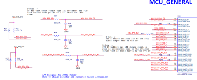
I have the below queries regarding the I2C interface
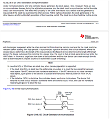
- Need information on the number of I2C interfaces available
- Termination of I2C interfaces when used as I2C interface and not used as I2C interface.
- Any additional recommendations / Guidelines
- Any concerns on Interfacing SoC Non-Failsafe I2C to devices that are powered before the SoC- Ex PMIC
- Any exception that are required to be considered when using the I2C interfaces.
- Can the I2C interface be used to interface with devices supporting SMBus or PMBus
Let me know your thoughts.