This thread has been locked.

If you have a related question, please click the "Ask a related question" button in the top right corner. The newly created question will be automatically linked to this question.

DRA821U: Schematic Review Request regarding USB interface

Part Number: DRA821U

Hi Jacinto Champ !

Can you please check if USB circuit was designed for appropriate working ?

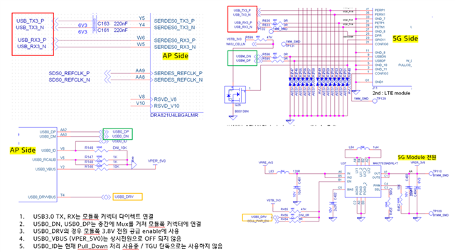
To help you with the translation in the attached picture,
1. USB 3.0 TX, RX connected directly to the connector on the 5G module.
2. USB0_DN and USB0_DP are connected to the module connector via MUX in the middle
3. The USB0_DRV is used as the 3.8V power supply enable signal for the 5G module.
4. USB0_VBUS (VPER_5V0) is not turned off at all times.
5. USB0_ID is currently processed by Pull_Down

  • 1. Are there DC-blocking caps on RX side?  I assume TX from processor are connected to RX of module (and visa-versa)?
    4. VBUS should be connected to USB0_DRV (using appropriate R-Divider).  USB0_DRV can still enable module as well.

  • Thanks for reply

    1. The USB 3.0 RX dc block cap is located inside the 5g module.

    4. Does it mean that I must turn off the power to VBUS using USB0_DRV?

        The VBUS is always on in our environment.

  • I would recommend connecting USBx_DRV and VBUS similar to how we connect to the USB Hub on our EVMs (since this is a tested configuration).   USBx_DRV is used to enable VBUS.  

    Using USBx_DRV to enable the 3.8V supply to module might be OK - power up timing might have to be adjusted to increase delay as supply is enabled and module powers up.  Our EVMs designs connect USBx_DRV directly to VBUS (via R-divider) for host config (to HUB), and so VBUS is available almost instantly after USBx_DRV is asserted.