Hi team,
When debugging MCU_SPI1 on J721S2, the chip select clock cannot be pulled high. The transmitted data waveform can be detected on MOSI, but the data cannot be received properly.
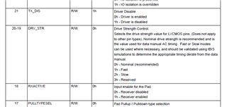
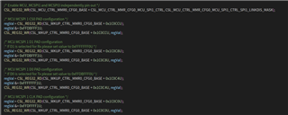
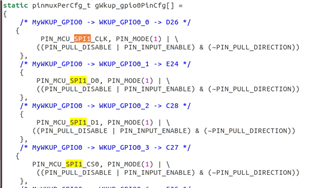
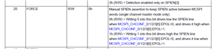
Customer follows Section 5.5.23.2 of TRM and write the MCU_SPI1_CTRL[SPI1_LINKDIS], MCU_SPI1_CLKSEL[MSTR_lb_CLKSEL], and SPI3_CLKSEL[MSTR_lb_CLKSEL] registers to 1. But MCU_SPI 1 chip select still cannot be pulled low. How to set it up with MCU_SPI1 to work properly standalone, not affected by SPI3?
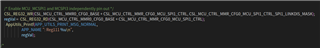
The code to write these 3 registers is as follows:
CSL_REG32_WR(CSL_CTRL_MMR0_CFG0_BASE + CSL_MCU_CTRL_MMR_CFG0_LOCK0_KICK0, 0x68EF3490);
CSL_REG32_WR(CSL_CTRL_MMR0_CFG0_BASE + CSL_MCU_CTRL_MMR_CFG0_LOCK0_KICK1,0xD172BC5A);
regVal = CSL_REG32_RD(CSL_CTRL_MMR0_CFG0_BASE + CSL_MCU_CTRL_MMR_CFG0_LOCK0_KICK0);
while ((regVal & 0x1) != 0x1U)
{
regVal = CSL_REG32_RD(CSL_CTRL_MMR0_CFG0_BASE + CSL_MCU_CTRL_MMR_CFG0_LOCK0_KICK0);
}
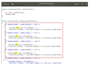
/* Enable MCU_MCSPI1 and MCSPI3 independently pin out */
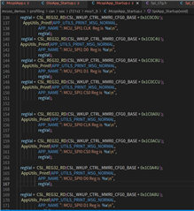
CSL_REG32_WR(CSL_MCU_CTRL_MMR0_CFG0_BASE + CSL_MCU_CTRL_MMR_CFG0_MCU_SPI1_CTRL, CSL_MCU_CTRL_MMR_CFG0_MCU_SPI1_CTRL_SPI1_LINKDIS_MASK);
regVal = CSL_REG32_RD(CSL_MCU_CTRL_MMR0_CFG0_BASE + CSL_MCU_CTRL_MMR_CFG0_MCU_SPI1_CTRL);
AppUtils_Printf(APP_UTILS_PRINT_MSG_NORMAL,
APP_NAME ": Reg111 %d\n",
regVal);
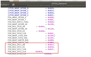
CSL_REG32_WR(CSL_WKUP_CTRL_MMR0_CFG0_BASE + CSL_MCU_CTRL_MMR_CFG0_MCU_TIMER5_CLKSEL + 16 ,1U);
regVal1 = CSL_REG32_RD(CSL_WKUP_CTRL_MMR0_CFG0_BASE + CSL_MCU_CTRL_MMR_CFG0_MCU_TIMER5_CLKSEL + 16 );
AppUtils_Printf(APP_UTILS_PRINT_MSG_NORMAL,
APP_NAME ": Reg222 %d\n",
regVal1);
CSL_REG32_WR(CSL_CTRL_MMR0_CFG0_BASE + CSL_MAIN_CTRL_MMR_CFG0_SPI3_CLKSEL + 16 ,1U);
regVal2 = CSL_REG32_RD(CSL_CTRL_MMR0_CFG0_BASE + CSL_MAIN_CTRL_MMR_CFG0_SPI3_CLKSEL + 16 );
AppUtils_Printf(APP_UTILS_PRINT_MSG_NORMAL,
APP_NAME ": Reg333 %d\n",
regVal2);
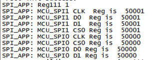
Only the MCU_SPI1_CTRL[SPI1_LINKDIS] register reads 1. The two registers MCU_SPI1_CLKSEL[MSTR_lb_CLKSEL], and SPI3_CLKSEL[MSTR_lb_CLKSEL] always read 0.
Could you help check this case? Thanks.
Best Regards,
Cherry