This thread has been locked.

If you have a related question, please click the "Ask a related question" button in the top right corner. The newly created question will be automatically linked to this question.

TDA4VM-Q1: Is a deviation from SPRACN9E (LPDDR4 board design guidelines) possible, regarding PCB trace characteristic impedance, On-Die termination and drive strength?

Part Number: TDA4VM-Q1


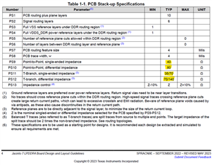
I have some questions regarding your recommendations about the PCB stackup, the LPDDR4 termination, drive strength and PCB trace characteristic impedance in your document “SPRACN9E – SEPTEMBER 2022 – REVISED MAY 2023”. See the following screen shot:

Due to project dependent PCB manufacturing constraints we have used a different stackup (12-layer) with increased impedances (50Ω/100Ω) for our prototype Jacinto LPDDR4 design. The design was successfully simulated and tested. We are now designing the final product and would rather like to transfer our prototype design and not follow the recommendation in your aforementioned document. Therefore my questions:


  1. Are we allowed to deviate from your recommended trace impedances and use 50Ω/100Ω instead (with appropriate changes to the Jacinto/LPDDR4 drive strength and ODT settings)? We will not reach the doubled impedances after the CA/CLK branches. But we will implement the highest possible impedance and simulate this.
    1. Are there any hints from you regarding this?
    2. Any precautions?
  2. What are the advantages of your low impedance design (besides the possibility to actually reach the doubled impedance after the CA/CLK branches)?
    1. What are the drawbacks regarding our higher impedance design?


I hope a TI Jacinto/LPDDR4 specialist can help us with this issue.

  • Yes - one of the advantage of using lower impedance is you can get closer to the target impedances for the CLK/CA branches.  The minimum trace width will likely drive the upper impedance of the branch and cannot be further raised.  Thus if the base trace impedance is raised, there will be larger impedance mis-match with branch.  Its impossible to predict how significant of an issue with will be - as functioning interface is dependent on many PCB design factors (signal loss/material, cross-talk, signal integrity, power noise, etc).  All will play a factor.  Are you operating LPDDR interface at maximum rate (4266Mbps)? 

    Our recommendation is to minimize risk is to follow our guidance/designs.  Its possible other design aspects/combinations will also work - as TI has not tested every possible combination. 

  • Yes, the minimum trace width will be the limiting factor for the impedances of the branch traces. And we will use the minimum trace width there and simulate the design. 


    No, we don't operate the interface at maximum speed, we will be operating the LPDDR4 interface at 3200Mbps. We will simulate and verify at 3200Mbps. But we will use LPDDR4 RAMs capable to run at 4266Mbps to add an additional safety layer to our design. What is your opinion on this?


    Are there any general advantages/disadvantages for or against your low impedance recommendation or our higher impedance design (besides the branch impedance issue)?


    I do agree with you about following your recommendation. But I'm faced here with a well-functioning prototype design which has been successfully simulated and tested. And now we will be working on the production version and have the choice to copy the previous (known working) design or integrate your impedance recommendations, which will impact the signal routing. What are your thoughts about this?

  • Using the higher speed devices operating at lower speeds should give you extra margin.  So yes this is recommended.  How does your existing trace width compare to the trace width on our EVM?  If trace is wider - the traces will be closer together (compared to our EVM) and could increase cross-talk.  Lowering the impedance means widening the traces (assuming no other PCB stackup changes) so again this could increase cross-talk, and likely not recommended if already at larger trace width.

    Well-functioning prototype design - how well have you tested?  Across temperature?  Have you tried increasing the DDR speed to see how much margin you might have?

    Most of the issues I've see are customers running at maximum speed (4266).  I've seen much fewer issues at lower speeds (3200, 3700), so I do think you have some flexibility in the PCB design.  Also not supply noise (CORE and DDR) will have impact on DDR performance, so make sure those are properly implemented on PCB (routing and decoupling).