A related question is a question created from another question. When the related question is created, it will be automatically linked to the original question.
If you have a related question, please click the "Ask a related question" button in the top right corner. The newly created question will be automatically linked to this question.
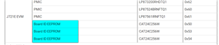
The J721E EVM is comprised different boards assembled together. A processor module (SOM), and common base board (CPB), and a add-on peripheral board (QSGMII). Each board has Configuration EEPROM to store EVM design information, revision, manufacturing date, etc. Each board has its own Board ID/Configuration EEPROM.
From J721E EVM User Guide:
The J721E EVM User Guide also includes the format of the EEPROM (Table 4-11)