This thread has been locked.

If you have a related question, please click the "Ask a related question" button in the top right corner. The newly created question will be automatically linked to this question.

TMS320C6205: Power-Up Sequencing

Part Number: TMS320C6205

Our customer sees C6205 fail to boot on some of their mass-production boards. The C6205 fails to boot when the rise time of the 3.3 V I/O supply is slow (about 10 ms) and succeeds when it is fast. They also confirmed by an A-B-A swap that the issue is not with the board but with C6205.

C6205 does not require specific power sequencing between the core supply and the I/O supply and specific rise time of each power supply, is that correct?

TMS320C6205 Fixed-Point Digital Signal Processor datasheet (Rev. G)
www.ti.com/.../tms320c6205.pdf
power-supply sequencing
"TI DSPs do not require specific power sequencing between the core supply and the I/O supply. However, systems should be designed to ensure that neither supply is powered up for extended periods of time if the other supply is below the proper operating voltage."

The /RESET is pulled-up to the 3.3V I/O supply, not pulled-down, and it is assert after power-up on their boards since the PLL requires a falling edge of /RESET to initialize the PLL engine, is that correct? Not so, it must be pulled-down?

Figure 5. External PLL Circuitry for Either PLL Multiply Modes or x1 (Bypass) Mode
NOTES:
E.
"At power up, the PLL requires a falling edge of RESET to initialize the PLL engine. It may be necessary to toggle reset in order to establish proper PLL operation."

Best regards,

Daisuke

  • Daisuke

    C6205 does not require specific power sequencing between the core supply and the I/O supply and specific rise time of each power supply, is that correct?

    The datasheet states:

    TI DSPs do not require specific power sequencing between the core supply and the I/O supply. However,
    systems should be designed to ensure that neither supply is powered up for extended periods of time if the other
    supply is below the proper operating voltage.

    I do not see any reference to rise time.

    The /RESET is pulled-up to the 3.3V I/O supply, not pulled-down, and it is assert after power-up on their boards since the PLL requires a falling edge of /RESET to initialize the PLL engine, is that correct? Not so, it must be pulled-down?

    Form the datasheet, which you already quoted, there must be a negative transition on the reset line in order to properly initialize the PLL engine.  So what is being done should correct.   Have you ensured that the reset timing is valid (p48 of datasheet)? 

    What are the symptoms of the failure? 

    I'm checking internally to see if there is additional knowledge on this. 

    --Paul

  • Hi Paul-san,

    Thank you for your reply.

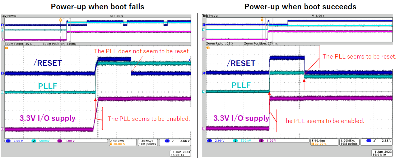
    Our customer suspected the PLL and checked the feedback output (PLLF) for the filter connection to see the difference between when the boot fails and when it succeeds. When the boot fails, the PLL does not seem to be reset.

    They also found that if the PLLV was powered from an independent 3.3V supply and raised after the other supplies had powered, the boot would no longer fail.

    Form the datasheet, which you already quoted, there must be a negative transition on the reset line in order to properly initialize the PLL engine.  So what is being done should correct.

    I suspect that the /RESET is pulled-up, is that really correct?

    Should the /RESET be pulled-down, released after power-up, and then asserted again to initialize the PLL?

    Best regards,

    Daisuke
  • Still checking on this and will get back to you as quickly as possible.

  • Hi Paul-san,

    Thank you for your suuport.

    How is the progress of what you are checking internally? What have you found out?

    Please give me an answer as soon as possible. Your prompt reply would be appreciated.

    Best regards,

    Daisuke

  • Should the /RESET be pulled-down, released after power-up, and then asserted again to initialize the PLL?

    This would be a experiment to try, however....

    The "timing requirements for reset" table has the following note for tw(RST):

    This parameter applies to CLKMODE x4, x6, x7, x8, x9, x10, and x11 only. The RESET signal is not connected internally to the Clock PLL circuit. The PLL requires a minimum of 250 μs to stabilize following device power up or after PLL configuration has been changed. During that time, RESET must be asserted to ensure proper device operation. See the clock PLL section for power up (specifically Figure 5, Note E) and for PLL lock times (Table 4).

    This would suggest that the reset is used to ensure proper device operation and not used for the PLL.

    I feel you need to understand why there is a difference in the 3.3v slew.  Is the 3.3v supply adequate enough to meet the connected devices?  Might be worth measuring the current draw between the two boards (good/bad).

    Does the PSU design satisfy the considerations detailed in the section titled "power-supply design considerations"?

    --Paul 

  • Hi Paul-san,

    Thank you for your reply.

    The "timing requirements for reset" table has the following note for tw(RST):

    This parameter applies to CLKMODE x4, x6, x7, x8, x9, x10, and x11 only. The RESET signal is not connected internally to the Clock PLL circuit. The PLL requires a minimum of 250 μs to stabilize following device power up or after PLL configuration has been changed. During that time, RESET must be asserted to ensure proper device operation. See the clock PLL section for power up (specifically Figure 5, Note E) and for PLL lock times (Table 4).

    This would suggest that the reset is used to ensure proper device operation and not used for the PLL.

    The fact that the /RESET signal is not used for the PLL seems to contradict the following note in the datasheet.

    Figure 5. External PLL Circuitry for Either PLL Multiply Modes or x1 (Bypass) Mode
    NOTES:
    E.
    "At power up, the PLL requires a falling edge of RESET to initialize the PLL engine. It may be necessary to toggle reset in order to establish proper PLL operation."

    Is the falling edge of the /RESET signal NOT required to initialize the PLL?

    Best regards,

    Daisuke

  • I agree this appears to be a contradiction. 

    However, reset is needed either way, and I believe you already have a falling edge in the design.  If possible, you could alway try the , pull-low option and implement such that there is a falling edge transition as you suggested earlier.  

    Any feedback on the 3.3v suggestions? 

    --Paul 

  • Hi Paul-san,

    Thank you for your reply.

    I agree this appears to be a contradiction. 

    However, reset is needed either way, and I believe you already have a falling edge in the design.  If possible, you could alway try the , pull-low option and implement such that there is a falling edge transition as you suggested earlier.  

    Could you clarify if the /RESET pin should be pulled-down?

    Could you check the /RESET pin on the C6205 evaluation module? Could you check the schematic?

    Any feedback on the 3.3v suggestions? 

    I have already suggested it to our customer.

    Since the considerations detailed in the section titled "power-supply design considerations" affect the 1.5V core power supply, I suggested to our customer to check the 1.5V core power supply as well.

    Best regards,

    Daisuke

  • Hi Paul-san,

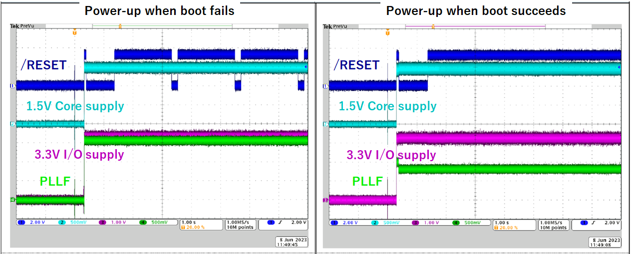
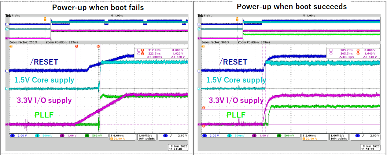
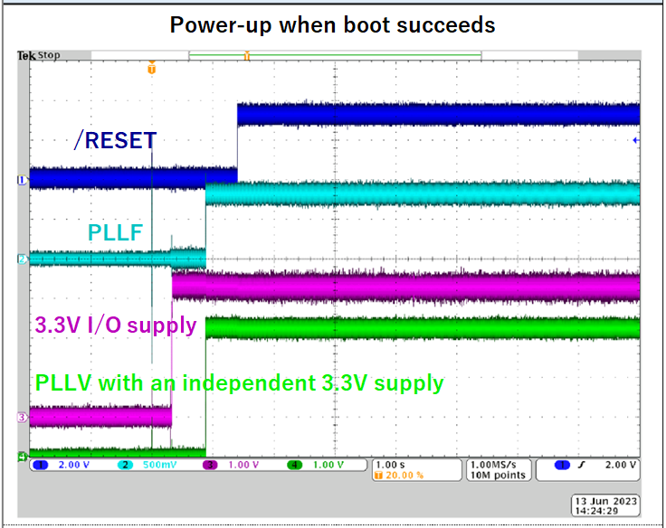
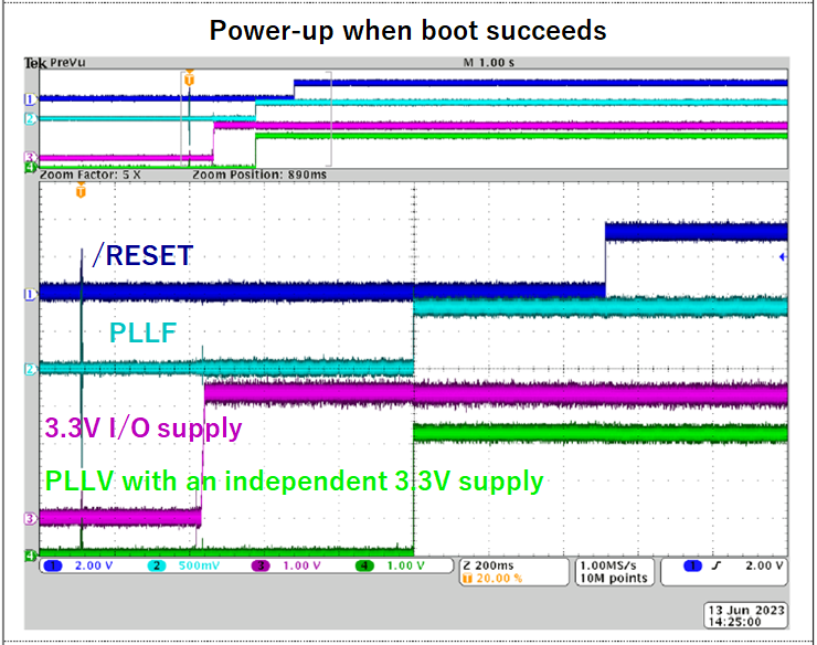
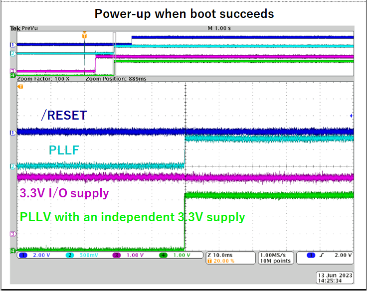
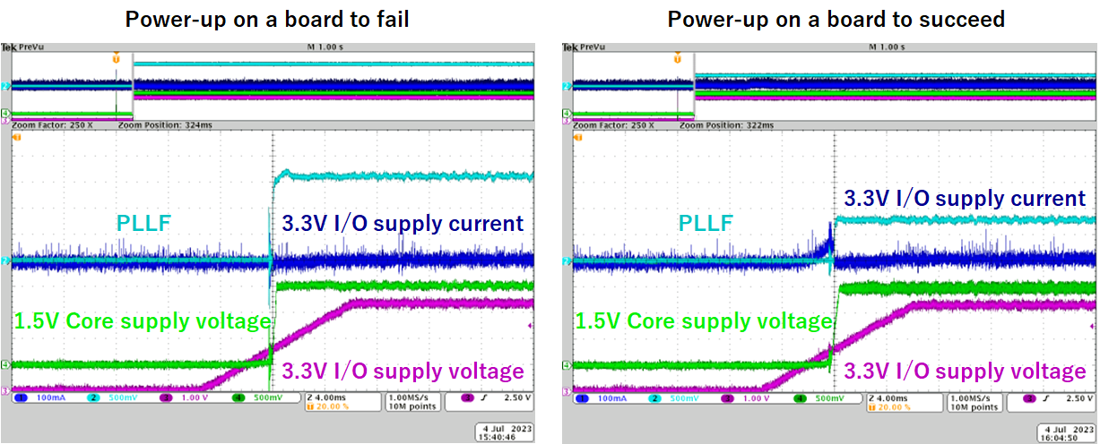
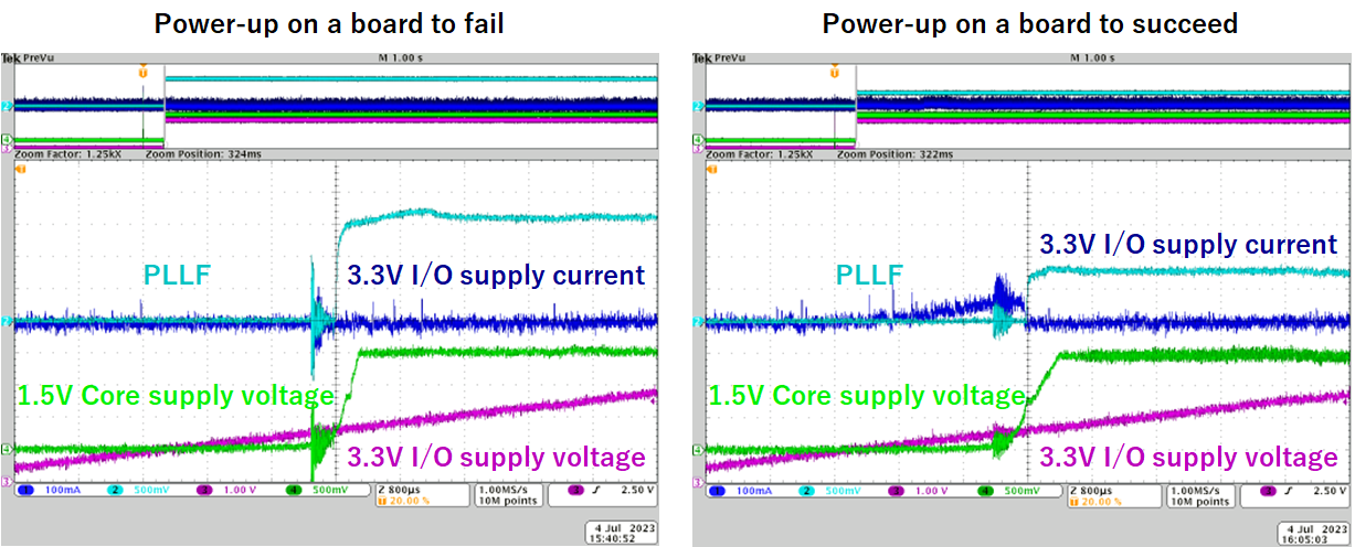
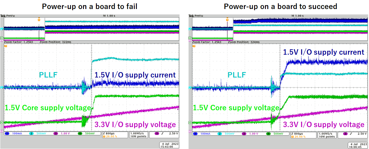
    The current consumption of each power supply has not yet been checked, but the voltage waveforms at power-up, including the 1.5V core power supply, have been checked.

    The PLLF voltage is different when the boot succeeds and when it fails.
    A similar issue has been posted in the following thread and our customer suspects that the failure follows the device.

    e2e.ti.com/.../3235246

    The voltage waveforms were also checked in the case where the PLLV was supplied from an independent 3.3V power supply.

    Best regards,

    Daisuke

  • I will look at these today.

    --Paul 

  • Hi Paul-san,

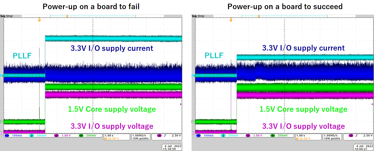
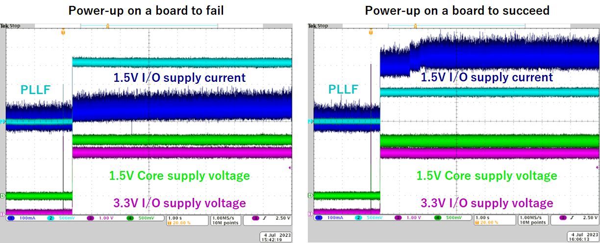
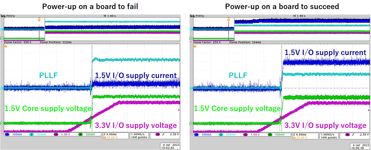
    The current consumption of each power supply at power-up has been checked.

    For 3.3V current consumption:

    For 1.5V current consumption:

    The PLLF voltage is different when the boot succeeds and when it fails.
    A similar issue has been posted in the following thread and our customer suspects that the failure follows the device.

    e2e.ti.com/.../3235246

    The issue posted in above thread has occurred in negative temperature environments, and our issue also occurs 100% of the time in negative temperature environments.

    Best regards,

    Daisuke

  • Thanks for the additional detailed information.

    So the 1.5v Core (mislabeled I/o?) current looks to be nominal (~300mA) when the device boots but only ~50mA when it does not boot - Probably due to the device not starting. 

    Difficult to tell what the 3.3v I/O current value is, but looks the same in both scenarios.

    I don't see anything obvious that would explain the slow ramp on the 3.3v I/O in the original scope shots.

    Since the customer has already done an A/B swap which shows the issue follows the processor. 

    Are all the board exhibiting the issues populated with processors from the same lot? Can you provide details of the markings?

    From where were the processors on the failing boards purchased?  

    Do the failing boards boot ok when not at a negative temperature? 

    How long has the design been in production? Were there any design changes or component updates  for the boards that have the issues? 

    I am checking to see if there was any conclusion to the linked thread. 

    -Paul 

  • Hi Paul-san,

    Thank you for your reply.

    Are all the board exhibiting the issues populated with processors from the same lot? Can you provide details of the markings?

    5 devices in about 300 devices have the issues and have the following two types of "Lot trace code".

    "C13-18CDLOW"
    "C13-02C2SGW"

    From where were the processors on the failing boards purchased?

    All devices are purchased from us.

    Do the failing boards boot ok when not at a negative temperature?

    They do not fail in non-negative temperature environments.

    How long has the design been in production? Were there any design changes or component updates  for the boards that have the issues? 

    All boards which have the design were manufactured in 2022.

    I am checking to see if there was any conclusion to the linked thread. 

    Our customer suspects that the devices with the above "Lot trace code" are defective.

    Best regards,

    Daisuke

  • Looks like we have had no device returns for Failure Analysis for this family of processor, so no conclusion for the linked thread. 

    Can you confirm the the 3.3v current is the same between a problem board and a good board? what are the actual current values?    There must be a reason why the ramp is different, typically this would be load. Understanding the root cause of the slow ramp sounds like the key.   

    Just to reconfirm, replacing the processor on a bad board resolves the issue and moving the processor from a bad board to a good board result in the good board failing? 

    --Paul

  • Hi Paul-san,

    Thank you for your reply.

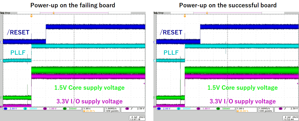
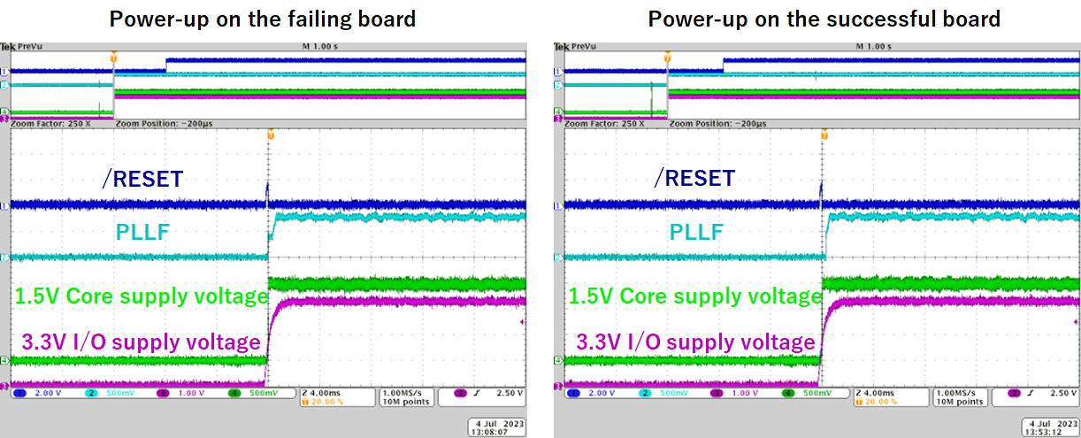
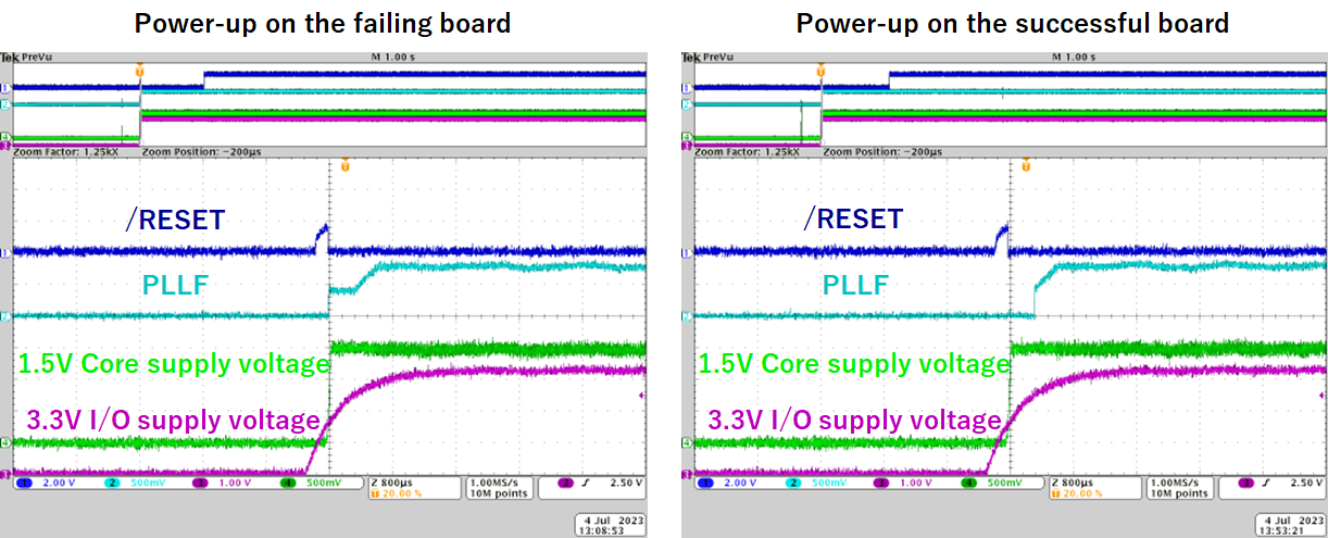
    The reason why the ramp is different is because 3.3V power is supplied from outside the DSP board and a 3.3V supply with a fast rise time was used for the tests.

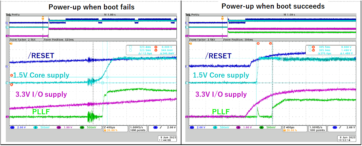
    The waveforms at power-up when using the 3.3V supply with a fast rise time are shown below.

    In this case, the failing board can also boot successfully, but the behaviour of the PLL feedback output (PLLF) differs from that of the successful board. PLLF appears to rise after the 3.3V supply on the successful board, but appears to rise with the 1.5V supply on the failing board.

    Does PLLF rising with a 1.5V supply indicate that the device is faulty?

    Best regards,

    Daisuke

  • So the measured 3.3v ramp  is the same for both good and bad boards?

    The only measured difference between good/bad is the PLLF? 

    Just to reconfirm, replacing the processor on a bad board resolves the issue and moving the processor from a bad board to a good board result in the good board failing? 

    Can you (re)confirm? 

    --Paul

  • Hi Paul-san,

    Thank you for your reply.

    So the measured 3.3v ramp  is the same for both good and bad boards?

    Yes.

    The only measured difference between good/bad is the PLLF? 

    Yes.

    Just to reconfirm, replacing the processor on a bad board resolves the issue and moving the processor from a bad board to a good board result in the good board failing? 

    Can you (re)confirm?

    It has been confirmed that replacing the processor on all bad boards resolves the issue. All replaced boards are working fine.

    I will ask our customer if they have confirmed that moving the processor from a bad board to a good board result in the good board failing.

    Best regards,

    Daisuke

  • I will ask our customer if they have confirmed that moving the processor from a bad board to a good board result in the good board failing.

    Pkease do check this as it completes the AB swap test 

    --Paul