


Hi,all
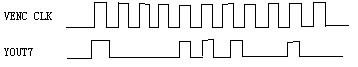
I want to use DM368 to decode H.264, and output from YCC16. Now, for test, I set all data in SDRAM to 0xFF, and then I use oscilloscope to check
the output signals (YOUT7-0,COUT7-0), and I suppose they would be all 1(high), but they are not.,like below :
I confuse about which registers I configure wrong, and hunger for your help.
Thanks.
My source code is shown below :
/******************************************************************/
// VENC clock domain get its clock from PLLC1SYSCLK6 : 54M
// I have set PINMUX1 right for COUT7-0
#define VIDEO_WIDTH 704
#define VIDEO_HEIGHT 576
#pragma DATA_SECTION(video_buffer, ".my_sect")
char video_buffer[VIDEO_WIDTH * VIDEO_HEIGHT * 2];// "video_buffer" Address is : 0x87B00000
void setup_vpbe(void)
{
unsigned int tmp_addr;
for (tmp_addr = 0; tmp_addr < (VIDEO_WIDTH * VIDEO_HEIGHT * 2); tmp_addr++)
{
video_buffer[tmp_addr] = 0xFF;
}
tmp_addr = (unsigned int)video_buffer;
tmp_addr >>= 5;
OSD_BASEPX = 0x00;
OSD_BASEPY = 0x00;
OSD_VIDWIN0XP = 0x00;
OSD_VIDWIN0YP = 0x00;
OSD_VIDWIN0XL = VIDEO_WIDTH;
OSD_VIDWIN0YL = VIDEO_HEIGHT;
OSD_VIDWIN0OFST = ((tmp_addr >> 23) << 9) | (VIDEO_WIDTH >> 4);//(0x08 << 9) for SDRAM address
OSD_VIDWINADH = (tmp_addr >> 16); // SDRAM start address higher 7bits
OSD_VIDWIN0ADR = tmp_addr; // VIDWIN0ADL SDRAM start address low 16bits
OSD_VIDWINMD = 0x01;
OSD_MODE = 0x0100;
OSD_MISCCTL = 0x00;
VENC_DCLKPTN0 = 0x01;
VENC_DCLKPTN1 = 0x00;
VENC_DCLKPTN2 = 0x00;
VENC_DCLKPTN3 = 0x00;
VENC_DCLKPTN0A = 0x02;
VENC_DCLKPTN1A = 0x00;
VENC_DCLKPTN2A = 0x00;
VENC_DCLKPTN3A = 0x00;
VENC_DCLKHSTT = 0x00;
VENC_DCLKHSTTA = 0x01;
VENC_DCLKHVLD = 0x00;
VENC_DCLKVSTT = 0x00;
VENC_DCLKVVLD = 0x00;
VENC_YCCCTL = 0x10;
VDAC_CONFIG = 0
| ( 0 << 19 ) // Output interrupt signal when TVOUT shorts to ground. Active high
| ( 0 << 5 ) // SD Video buffer mode
| ( 0 << 4 ) // Disable TVINT circuit enable signal
| ( 0 << 3 ) // Power down control for SD Video Buffer in Normal
| ( 0 << 2 ) // Power down mode control for CH-C
| ( 0 << 1 ) // Power down mode control for CH-B
| ( 0 << 0 ) // Power down mode control for CH-A
;
VPSS_CLKCTL = 0
| ( 0 << 7 ) // Config/DMA bus clock versus VPSS clock ratio 1:2
| ( 0 << 5 ) // PLLC1SYSCLK6 as 27/74.25 MHz input source
| ( 1 << 4 ) // Enabled Video DAC clock
| ( 1 << 3 ) // Enabled VPBE/Video encoder clock
| ( 0 << 2 ) // Diable VENC clock mux and receive normal PCLK
| ( 0 << 0 ) // VPSS clock selection Use input set by VENC_CLK_SRC
;
VPSS_VPBE_CLK_CTRL = 0
| ( 0 << 7 ) // LDC memory clock select 0: OSD module 1: ARM, has access to memory
| ( 0 << 6 ) // OSD memory clock select 0: OSD module 1: ARM, has access to memory
| ( 0 << 5 ) // Reserved
| ( 0 << 4 ) // Reserved
| ( 1 << 3 ) // Enable LDC clock
| ( 0 << 2 ) // VENC clock select ENC_CLOCK * 1
| ( 0 << 1 ) // Reserved
| ( 1 << 0 ) // Enable OSD, VENC clock
;
VENC_CLKCTL = 0
| ( 0 << 8 ) // Diable Clock for gamma correction table
| ( 1 << 4 ) // Enable Clock for digital LCD controller
| ( 1 << 0 ) // Enable Clock for video encoder
;
VENC_VMOD = 0
| ( 0 << 12 ) // YCC16
| ( 1 << 9 ) // Interlace
| ( 0 << 8 ) // SDTV mode
| ( 1 << 6 ) // PAL
| ( 0 << 5 ) // Master mode
| ( 1 << 4 ) // Not NTSC/PAL/HDTV timing
| ( 0 << 3 ) // Blanking enable
| ( 1 << 1 ) // Composite output enable
| ( 1 << 0 ) // Video encoder enable
;
VENC_VDPRO = 0x0000; // Normal mode, not colorbars
VENC_DACTST = 0x0000; // Power on DACs
VENC_DACSEL = 0x0543; // Component out on DACs
VENC_HSPLS = 0 | ( 1 << 0 ) ;
VENC_VSPLS = 0 | ( 1 << 0 ) ;
VENC_HINTVL = 0 | ( 1449 << 0 ) ;
VENC_HSTART = 0 | ( 0 << 0 ) ;
VENC_HVALID = 0 | ( 1450 << 0 ) ;
VENC_VINTVL = 0 | ( 624 << 0 ) ;
VENC_VSTART = 0 | ( 0 << 0 ) ;
VENC_VVALID = 0 | ( 625 << 0 ) ;
VENC_HSDLY = 0 | ( 0 << 0 ) ;
VENC_VSDLY = 0 | ( 0 << 0 ) ;
VENC_VIOCTL = 0
| ( 0 << 14 ) // VCLK output polarity Non-inverse
| ( 1 << 13 ) // VCLK output enable
| ( 0 << 12 ) // VCLK pin output enable
| ( 0 << 8 ) // HSYNC/VSYNC pin I/O control Output
| ( 0 << 4 ) // Digital data output mode Normal output
| ( 0 << 3 ) // Swaps YOUT/COUT pins Normal output
| ( 0 << 2 ) // YOUT/COUT pin DC output mode Normal output
| ( 0 << 0 ) // YOUT/COUT I/O Direction Output
;
VENC_SYNCCTL = 0
| ( 0 << 14 ) // OSD vsync delay Not delay
| ( 0 << 12 ) // External field detection mode Latch external field at external vsync rise edge
| ( 0 << 11 ) // External field input inversion Non-inverse
| ( 0 << 10 ) // External sync select HSYNC/VSYNC pin
| ( 0 << 9 ) // External vertical sync input polarity Active H
| ( 0 << 8 ) // External horizontal sync input polarity Active H
| ( 0 << 7 ) // Composite sync output polarity Active H
| ( 0 << 6 ) // Composite sync output enable Off
| ( 0 << 5 ) // Output sync select Normal
| ( 0 << 4 ) // VSYNC pin output signal select Vertical sync signal
| ( 0 << 3 ) // Vertical sync output polarity Active H
| ( 0 << 2 ) // Horizontal sync output polarity Active H
| ( 1 << 1 ) // Vertical sync output enable On
| ( 1 << 0 ) // Horizontal sync output enable On
;
VENC_LCDOUT = 0
| ( 0 << 8 ) // Output enable signal selection LCD Output Enable signal
| ( 0 << 7 ) // Field ID output polarity Non-inverse
| ( 0 << 6 ) // PWM output pulse polarity Active H
| ( 0 << 5 ) // PWM output control enable Off
| ( 0 << 4 ) // LCD_AC output control enable Off
| ( 0 << 3 ) // Bright output polarity Active H
| ( 0 << 2 ) // Bright output control enable Off
| ( 0 << 1 ) // LCD_OE output polarity Active H
| ( 1 << 0 ) // LCD_OE output control enable On
;
VENC_DCLKCTL = 0
| ( 0 /*1*/ << 15 ) // DCLK internal mode enabled
| ( 0 << 12 ) // DCLK output offset 0
| ( 1 << 11 ) // DCLK pattern mode Enable
| ( 0 << 10 ) // DCLK mask enable Off
| ( 0 << 9 ) // DCLK output divide control Divide by 1
| ( 0 << 8 ) // Internal DCLK divide control Divide by 1
| ( 0 << 0 ) // DCLK pattern valid bit width
;
}
/******************************************************************/
Archer
7/28/2011 16:46