Other Parts Discussed in Thread: AM6442
Hello,
I am using AM6442 board, on a no-RTOS, bare-metal system on Windows.
My final goal is to use GPMC to connect to an external FPGA and use the UDMA for transfers.
Now as the first step, I am trying to configure the registers and clock for GPMC. I did the following steps:
I enabled the clock for GPMC:
SOC_moduleClockEnable(TISCI_DEV_GPMC0, 1);
I set the configuration registers for GPMC. Since no GPMC driver is provided for AM64x, Instead, based on this link I used the low-level GPMC driver from AM65x. So I didn't need to define the addresses and masks for registers. https://e2e.ti.com/support/processors-group/processors/f/processors-forum/1031271/processor-sdk-am64x-mcu_plus_sdk_am64x_08_00_00_21-gpmc-driver-header-files-missing
Then I tried to read and set the clock frequency for GPMC. Based on the TRM there is only two clock source possible for the GPMC FCLK: PLL0_HSDIV3 or PLL2_HSDIV7.
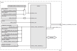
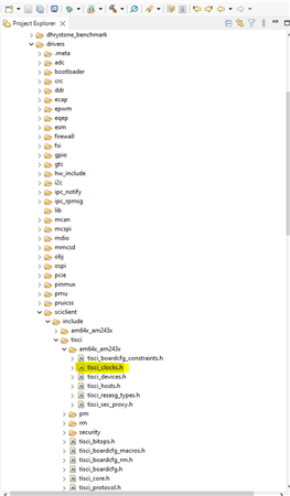
However in tisci_clocks.h 5 sources defined for GPMC:
Based on the above explanation, here are my questions:
1. I believe CLKB is the output clk of GPMC (2). HSDIV3 and HSDIV7 are the inputs to the mux(5 and 6). ICLK (interface clk) is the same as clk_In (3). and FCLK_MUX_IN (4) is the output of the mux.Do you confirm that?
2. I tried to read the frequency of these different clocks and somehow set the frequency of the final FCLK, but the read values don't make sense. Also, it doesn't change the frequencies. Why?
status = SOC_moduleSetClockFrequency(
TISCI_DEV_GPMC0,
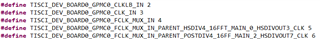
TISCI_DEV_BOARD0_GPMC0_FCLK_MUX_IN,
10000000
); // status is successful but it doesn't change the frequency
status = SOC_moduleSetClockFrequency(
TISCI_DEV_GPMC0,
TISCI_DEV_BOARD0_GPMC0_FCLK_MUX_IN_PARENT_HSDIV4_16FFT_MAIN_0_HSDIVOUT3_CLK,
10000000
); // statys is fail.
status= Sciclient_pmGetModuleClkFreq(TISCI_DEV_GPMC0,
TISCI_DEV_BOARD0_GPMC0_FCLK_MUX_IN,
&freqHz,
SystemP_WAIT_FOREVER); // reads 250 MHz
status= Sciclient_pmGetModuleClkFreq(TISCI_DEV_GPMC0,
TISCI_DEV_BOARD0_GPMC0_FCLK_MUX_IN_PARENT_HSDIV4_16FFT_MAIN_0_HSDIVOUT3_CLK,
&freqHz,
SystemP_WAIT_FOREVER); // reads 0 Hz
status= Sciclient_pmGetModuleClkFreq(TISCI_DEV_GPMC0,
TISCI_DEV_BOARD0_GPMC0_FCLK_MUX_IN_PARENT_POSTDIV4_16FF_MAIN_2_HSDIVOUT7_CLK,
&freqHz,
SystemP_WAIT_FOREVER); // reads 0 Hz
status= Sciclient_pmGetModuleClkFreq(TISCI_DEV_GPMC0,
TISCI_DEV_BOARD0_GPMC0_CLK_IN,
&freqHz,
SystemP_WAIT_FOREVER); // reads 0 Hz
status= Sciclient_pmGetModuleClkFreq(TISCI_DEV_GPMC0,
TISCI_DEV_BOARD0_GPMC0_CLKLB_IN,
&freqHz,
SystemP_WAIT_FOREVER); // reads 100 MHz
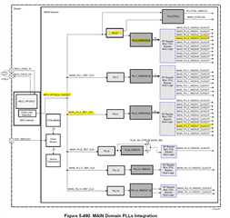
3. based on the following clock tree, I checked PLL0 and PLL0_HSDIV3 and they are both enable and their outputs are enabled (they are all containing the default values set by SYSFW). Based on my calculation based on the data dump of the registers(provided in the table). the HSDIV3_CLKOUT should be 133 MHz. But what I see by using the Sciclient_pmGetModuleClkFreq function is 0 Hz. Why? Is this function supposed to work for GPMC on AM64x?
|
Register name |
Address |
Value in application |
Fields |
|
|
0x00680000 |
61801001 |
|
|
|
0x00680008 |
03FF0801 |
|
|
|
0x00680010 |
68EF3491 |
|
|
|
0x00680014 |
D172BC5A |
|
|
PLL0_CTRL |
0x00680020 |
00018011 |
Bit 0, DAC_EN = 1: Fractional NC DAC is enabled |
|
Bit 1, DSM_EN = 0 :Delta sigma modulator is disabled |
|||
|
Bit 4, CLK_POSTDIV_EN =1 : post divide enabled. FOUTPOSTDIV, 4-phase and synchronous clocks are enabled |
|||
|
Bit 5, CLK_4PH_EN = 0 : 4-phase dividers disabled. |
|||
|
Bit 8, INTL_BYP_EN = 0 :Output clocks are derived from VCO clock. |
|||
|
Bit 15, PLL_EN = 1: PLL is enabled |
|||
|
Bit 16, BYP_ON_LOCKLOSS =1 : switch to ref clock source when PLL losses lock |
|||
|
Bit 31, BYPASS_EN = 0. |
|||
|
PLL0_STAT |
0x00680024 |
00000001 |
Bit 0, Lock =1 : PLL is locked |
|
PLL0_FREQ_CTRL_0 |
0x00680030 |
00000050 |
Bits [11-0], FB_DIV_INT = 80: divide by 80 |
|
PLL0_FREQ_CTRL_1 |
0x00680034 |
00000000 |
Bits [23-0], FB_DIV_FRAC = 0 : |
|
PLL0_DIV_CTRL |
0x00680038 |
01020001 |
Bits [5-0], REF_DIV= 1 : Divide by 1 |
|
Bits[18-16], POST_DIV1 : Divide by 2 |
|||
|
Bits[26-24], POST_DIV2 : Divide by 1 |
|||
|
PLL0_SS_CTRL |
0x00680040 |
80000000 |
|
|
PLL0_SS_SPREAD |
0x00680044 |
00010001 |
|
|
PLL0_CAL_CTRL |
0x00680060 |
80070F73 |
|
|
PLL0_CAL_STAT |
0x00680064 |
80000F73 |
|
|
PLL0_HSDIV_CTRL0 |
0x00680080 |
00008003 |
Bits[6-0], HSDIV : CLKOUT divider value (HSDIV+1) => divide by 4. Bit 8, SYNC_DIS = 0 : Changes to DIV value synchronized to prevent glitches. Bit 15, CLKOUT_EN = 1 : enable Bit 31, RESET = 0 |
|
PLL0_HSDIV_CTRL1 |
0x00680084 |
00008009 |
Bits[6-0], HSDIV : CLKOUT divider value (HSDIV+1) => divide by 10. Bit 8, SYNC_DIS = 0 : Changes to DIV value synchronized to prevent glitches. Bit 15, CLKOUT_EN = 1 : enable Bit 31, RESET = 0 |
|
PLL0_HSDIV_CTRL2 |
0x00680088 |
00008018 |
Bits[6-0], HSDIV : CLKOUT divider value (HSDIV+1) => divide by 25. Bit 8, SYNC_DIS = 0 : Changes to DIV value synchronized to prevent glitches. Bit 15, CLKOUT_EN = 1 : enable Bit 31, RESET = 0 |
|
PLL0_HSDIV_CTRL3 |
0x0068008C |
0000800E |
Bits[6-0], HSDIV : CLKOUT divider value (HSDIV+1) => divide by 15. Bit 8, SYNC_DIS = 0 : Changes to DIV value synchronized to prevent glitches. Bit 15, CLKOUT_EN = 1 : enable Bit 31, RESET = 0 |
|
PLL0_HSDIV_CTRL4 |
0x00680090 |
00008007 |
Bits[6-0], HSDIV : CLKOUT divider value (HSDIV+1) => divide by 8. Bit 8, SYNC_DIS = 0 : Changes to DIV value synchronized to prevent glitches. Bit 15, CLKOUT_EN = 1 : enable Bit 31, RESET = 0 |
|
PLL0_HSDIV_CTRL5 |
0x00680094 |
00008004 |
Bits[6-0], HSDIV : CLKOUT divider value (HSDIV+1) => divide by 5. Bit 8, SYNC_DIS = 0 : Changes to DIV value synchronized to prevent glitches. Bit 15, CLKOUT_EN = 1 : enable Bit 31, RESET = 0 |
|
PLL0_HSDIV_CTRL6 |
0x00680098 |
00008004 |
Bits[6-0], HSDIV : CLKOUT divider value (HSDIV+1) => divide by 5. Bit 8, SYNC_DIS = 0 : Changes to DIV value synchronized to prevent glitches. Bit 15, CLKOUT_EN = 1 : enable Bit 31, RESET = 0 |
|
PLL0_HSDIV_CTRL7 |
0x0068009C |
00008004 |
Bits[6-0], HSDIV : CLKOUT divider value (HSDIV+1) => divide by 5. Bit 8, SYNC_DIS = 0 : Changes to DIV value synchronized to prevent glitches. Bit 15, CLKOUT_EN = 1 : enable Bit 31, RESET = 0 |
|
PLL0_HSDIV_CTRL8 |
0x006800A0 |
00008007 |
Bits[6-0], HSDIV : CLKOUT divider value (HSDIV+1) => divide by 8. Bit 8, SYNC_DIS = 0 : Changes to DIV value synchronized to prevent glitches. Bit 15, CLKOUT_EN = 1 : enable Bit 31, RESET = 0 |
|
PLL0_HSDIV_CTRL9 |
0x006800A4 |
00008002 |
Bits[6-0], HSDIV : CLKOUT divider value (HSDIV+1) => divide by 3. Bit 8, SYNC_DIS = 0 : Changes to DIV value synchronized to prevent glitches. Bit 15, CLKOUT_EN = 1 : enable Bit 31, RESET = 0 |