This thread has been locked.

If you have a related question, please click the "Ask a related question" button in the top right corner. The newly created question will be automatically linked to this question.

LP-AM263: problem with GPIO pin assignment by sysconfig

Part Number: LP-AM263
Other Parts Discussed in Thread: SYSCONFIG

The gpio_led_blink example in the sdk works fine for the red led on my LP-AM263.

To test GPIO assignment I modified this basic example.

I connected an external led to pin 33 on booster pack header J4 and

used sysconfig to assign PRO_PRU0_GPIO0 to it which is

GPIO93 in standard multiplexing mode 7.

This modified blink program seems to work fine in processor memory, but the external led doesn't blink.

The external led works fine when it is powered by another 3.3V power supply.

But not here on pin 33 at booster pack header J4 with this program.

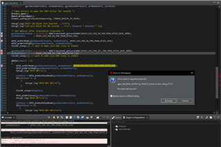
The multiplexing configuration made by sysconfig in ti_pinmux_config.c is:


static Pinmux_PerCfg_t gPinMuxMainDomainCfg[] = {
/* GPIO0 pin config */
/* GPIO26 -> UART0_CTSn (B7) */
{
PIN_UART0_CTSN,
( PIN_MODE(7) | PIN_PULL_DISABLE | PIN_SLEW_RATE_HIGH | PIN_QUAL_SYNC | PIN_GPIO_R5SS0_0 )
},
/* GPIO0 pin config */
/* GPIO93 -> PR0_PRU0_GPIO0 (K17) */
{
PIN_PR0_PRU0_GPIO0,
( PIN_MODE(7) | PIN_PULL_DISABLE | PIN_SLEW_RATE_HIGH | PIN_QUAL_SYNC | PIN_GPIO_R5SS0_0 )
},
/* GPIO0 pin config */
/* GPIO94 -> PR0_PRU0_GPIO1 (K18) */
{
PIN_PR0_PRU0_GPIO1,
( PIN_MODE(7) | PIN_PULL_DISABLE | PIN_SLEW_RATE_HIGH | PIN_QUAL_SYNC | PIN_GPIO_R5SS0_0 )
},
/* GPIO0 pin config */
/* GPIO96 -> PR0_PRU0_GPIO3 (J17) */
{
PIN_PR0_PRU0_GPIO3,
( PIN_MODE(7) | PIN_PULL_DISABLE | PIN_SLEW_RATE_HIGH | PIN_QUAL_SYNC | PIN_GPIO_R5SS0_0 )
},

/* UART0 pin config */
/* UART0_RXD -> UART0_RXD (A7) */
{
PIN_UART0_RXD,
( PIN_MODE(0) | PIN_PULL_DISABLE | PIN_SLEW_RATE_LOW )
},
/* UART0_TXD -> UART0_TXD (A6) */
{
PIN_UART0_TXD,
( PIN_MODE(0) | PIN_PULL_DISABLE | PIN_SLEW_RATE_LOW )
},

{PINMUX_END, PINMUX_END}
};

If processor pad K17 is connected to pin 33 at booster pack header J4 then this should work.

Why is this not working?

Help would be very much appreciated.

Kind regards

Robert

  • Hello Robert,

    Hmm... I don't have a LaunchPad immediately available to test but I feel the documentation and schematic are slightly mismatched.

    The PR0_PRU0_GPIO0 output is coming from the Mux and you removed all the code associated with controlling the mux. From the schematic what I see is that you need to set the mux to be enabled and then selected high so the PR0_PRU0_GPIO0 signal is what passes through to the BoosterPack header.

    This based on Page 11 of the schematic:

    However the document implies that PR0_PRU0_GPIO0 is passed through by default. That doesn't seem to be what the schematic indicates.

    Can you check if adding the mux control and setting the mux select high will allow the LED to blink? If so I will review the documentation with our team to make that part of the table more intuitive to understand.

    Best Regards,

    Ralph Jacobi

  • Hello Ralph,

    Thank you for your advice. I expected sysconfig to activate mux control together with the mux settings.

    I'm new to sysconfig and CCS so please be patient with me.

    How do I activate mux control for  PR0_PRU0_GPIO0?

    Kind regards

    Robert

  • Hi Robert,

    So the default gpio_led_blink example for AM263 LaunchPad covers that too.

    You'd have to restore the pins in SysConfig but the code used to control the Mux is like this:

        /* Get address after translation translate */
        gpioBaseAddr_en = (uint32_t) AddrTranslateP_getLocalAddr(AM263_U52_MUX_EN_GPIO58_BASE_ADDR);
        pinNum_en      = AM263_U52_MUX_EN_GPIO58_PIN;
    
        GPIO_setDirMode(gpioBaseAddr_en, pinNum_en, AM263_U52_MUX_EN_GPIO58_DIR);
        GPIO_pinWriteHigh(gpioBaseAddr_en, pinNum_en);
        ClockP_sleep(1); /* just make sure MUX route is stable */
    
        gpioBaseAddr_sel = (uint32_t) AddrTranslateP_getLocalAddr(AM263_U52_MUX_SEL_GPIO63_BASE_ADDR);
        pinNum_sel      = AM263_U52_MUX_SEL_GPIO63_PIN;
    
        GPIO_setDirMode(gpioBaseAddr_sel, pinNum_sel,AM263_U52_MUX_SEL_GPIO63_DIR);
        GPIO_pinWriteHigh(gpioBaseAddr_sel, pinNum_sel);
        ClockP_sleep(1); /* just make sure MUX route is stable */

    Best Regards,

    Ralph Jacobi

  • Hello Ralph,

    Thank you for this example. I tried to adapt it to my program an recieved these errors:

    This is my CCS project. It is a copy of the blink example.

    gpio_led_blink_am263x-lp_r5fss0-0_nortos_ti-arm-clang_V1.0.7.zip

    Please have a look why this not working.

    Thank you in advance!

    Robert

  • Hello Ralph,

    Sorry I misunderstood your answer and what you wanted me to do.

    I used a multimeter and checked the logic voltages on DDR-Switch U23.

    By default (no program running) DDR-Switch U23 input EN on pin 8 is HIGH

    and SEL1 and SEL2 on Pin 9 and 10 are LOW on my LP-AM263.

    PR0_PRU0_GPIO1 arrives on A1(and toggles while the blink program is running)

    and is routed to B1 on pin 39 instead of C1 on pin 40 which would lead to header J4 pin 32

    where I need it.

    Yes, all PR0_PRU0_GPIOx are by default routed by DDR-Switch U23 to B-outputs

    instead of C-outputs, which deactivates all booster pack pin headers for GPIOs.

    I understand that you tried to switch SEL1 and SEL2 to HIGH in your software example.

    Unfortunately your code example throws up errors when I compile it:

    Is there another way to get SEL1 and SEL2 on U23 to HIGH?

    Kind regards 

    Robert

  • Hello Robert,

    I didn't highlight this as clearly as I could have but

    You'd have to restore the pins in SysConfig

    What this means is you need to go in SysConfig and add back the removed configurations for those IO. Or it may be easier to just re-load a fresh gpio_led_blink example and then make your modifications to it.

    Without SysConfig setup for the Mux pins, the code I shared won't compile.

    Best Regards,

    Ralph Jacobi

  • Hello Ralph,

    The GPIO examples in the LP-263 SDK use an onboard led on GPIO26 and an onboard switch.

    In both examples there are no GPIOs configurations in Sysconfig for EN and SEL1/2 on DDR switch U23. 

    There is nothing for me to restore, because Sysconfig GPIOs for EN and SEL1/2 don't exist in your code examples.

    Please talk to your SDK team to include samples that work for using the GPIO pins on the boosterpack headers.

    This was a real hurdle for me, because I expected the GPIO pins on the boosterpack headers to be connected to the cpu ball pads by default.

    And I din't find any hints in the cpu documentation or sdk examples that would make me consider switching EN and SEL1/2 to HIGH on

    DDR switch U23 via Sysconfig and GPIO outputs to switch the disconnected GPIO pins on the LP-AM263 boosterpack headers to the cpu pads.

    Please add some instructions explaining this important feature of the LP-AM263 to the boosterpack signal chart in the launchpad box.

    What I still don't understand is why you name the additional GPIOs AM263_U52_MUX_EN_GPIO58 and AM263_U52_MUX_SEL_GPIO63.

    On LP-AM263 the DDR switch is called U23 and not U52. This was also confusing for me. 

    In order to use GPIO pins on the boosterpack headers of the LP-AM263 users need to set up two additional GPIOs in Sysconfig:

    EN on DDR switch U23 needs a GPIO output called AM263_U52_MUX_EN_GPIO58 assigned to pin EPWM7_B/F1

    SEL1/2 on DDR switch U23 needs a GPIO output called AM263_U52_MUX_SEL_GPIO63 assigned to pin EPWM10_B/J3

    Both outputs need to be switched to HIGH in the user program to connect the GPIO pins on LP-AM263 boosterpack headers to the cpu pads

    Thank you again for your help.

    Kind regards

    Robert

  • Hello Ralph,

    in default cpu mux mode 7 the external LED on PR0_PRU0_GPIO1 still did not blink.

    I had to set up cpu mux mode 0 for PR0_PRU0_GPIO1 with an additional configuration in the user program.

  • Hello Ralph,

    There was a typing error in my user program. I apologize. 

    In default cpu mux mode 7 external LEDs on PR0_PRU0_GPIOx work just fine.

    Would you like me to upload my working example for GPIO pins on LP-AM263?

    Thank you again for your patience and for your advice

    Kind regards 

    Robert

  • Hi Robert,

    Thanks for your candid feedback... I'll take a lot of fault for complicating this issue due to two bad assumptions on my end.

    In both examples there are no GPIOs configurations in Sysconfig for EN and SEL1/2 on DDR switch U23. 

    This was on me, I could have sworn I had imported a new project that day and that's where I saw them but now I've realized I had not done that and I had added that code for a past issue. So that's 100% on me for telling you something was present that was not. Had I realized there wasn't a quick example for that, I would have put together a proper example and shared it inside of giving you misleading instructions. Also in hindsight, I should have just provided the associated .c file and .sysconfig files so you had quick references regardless.

    Please talk to your SDK team to include samples that work for using the GPIO pins on the boosterpack headers.

    Yes looking back at this thread, it's pretty clear the whiff on our end... I'll raise this request for SDK improvement and will also try in the interim to put together a more comprehensive example for doing the same just to post to E2E.

    And I din't find any hints in the cpu documentation or sdk examples that would make me consider switching EN and SEL1/2 to HIGH on

    DDR switch U23 via Sysconfig and GPIO outputs to switch the disconnected GPIO pins on the LP-AM263 boosterpack headers to the cpu pads.

    Please add some instructions explaining this important feature of the LP-AM263 to the boosterpack signal chart in the launchpad box.

    I will review what documentation we have and don't have regarding this both in the BoosterPack User's Guide and the SDK documentation.

    What I still don't understand is why you name the additional GPIOs AM263_U52_MUX_EN_GPIO58 and AM263_U52_MUX_SEL_GPIO63.

    On LP-AM263 the DDR switch is called U23 and not U52. This was also confusing for me. 

    So this one is a bit of a mixed issue...

    • The two muxes share the same I/O for the EN line, so we should probably just not name a specific chip
    • Because I knew the enable was right. that led me to assuming the mux select from that example was for the right one for what you needed, but in reality the code I had seen for the GPIO LED Blink was controlling the U52 mux and you needed the U23 mux.
      • I imagine if we have an example controlling the U23 mux, the MUX SEL for that would be labelled accurately, but it likely wouldnt label the MUX EN accurately so I'll submit feedback for that.
    • If I had recognized that properly, I would have instead explained that while the process is similar, you'd need to reflect the pin for the U23 mux which the select pin there is GPIO64 instead of GPIO63.
    Would you like me to upload my working example for GPIO pins on LP-AM263?

    I'm sure other community members could use such a project if they run into similar issues. 

    While I am glad that you were able to get this working, I'm disappointed that I wasn't able to enable you sooner. I apologize for my own missteps here that dragged this out longer than needed.

    Best Regards,

    Ralph Jacobi

  • Hello Ralph,

    This version of the gpio_led_blink example works on my LP-AM263.

    gpio_led_blink_am263x-lp_r5fss0-0_nortos_ti-arm-clang_V1.1.1.zip

    I appreciate your help.

    Kind regards

    Robert