This thread has been locked.

If you have a related question, please click the "Ask a related question" button in the top right corner. The newly created question will be automatically linked to this question.

TDA4VH-Q1: demo pcb design

Part Number: TDA4VH-Q1

In the PCB design file of the DEMO, the T-trace end of the CKP/N of LPDDR near the LPDDR particle PIN pin trace does not take the differential trace, what is the reason for not taking the differential line?

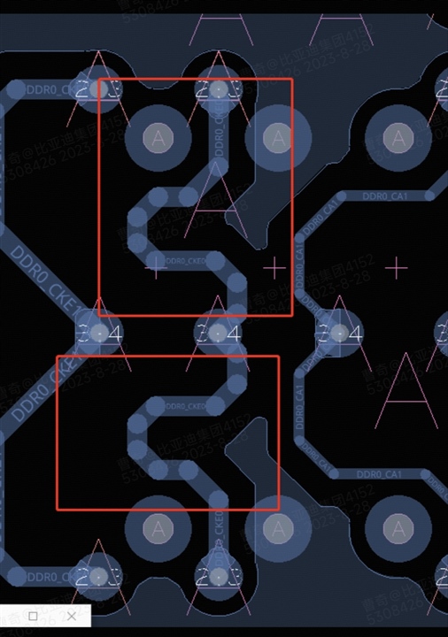
In the PCB design file of DEMO, the end of the T-trace of the CKE0/CKE1 of LPDDR is deliberately long, and the trace of the LPDDR particle PIN pin is deliberately long, and the shortest path is not taken. What is the reason for winding the end of the LPDDR particle PIN pin?

  • For the CLK routing, the T'branched portion of the trace should be twice the impedance of the original trace.  It unlikely that impedance can be achieved (due to minimum trace width requirements of the board), but closest achievable impedance should be goal.  I don't have the actual impedance calculations for this design (for these small segments), but goal for trace segments was stated (2x differential impedance of base trace segments).  Also very important is equal distance of length of each T-branch segment.  This is because the trace splits, and design is to have equal distances on each branch so any reflections are aligned/canceled. 

    For the serpentine of the CKE signal, this is done to match overall signal delay/skew on a signal to rest of the signals in an assigned bus class.  Again, since the signal is T-branched, similar design considerations for impedance control and branch length are requried.