This thread has been locked.

If you have a related question, please click the "Ask a related question" button in the top right corner. The newly created question will be automatically linked to this question.

TDA4VM-Q1: LPDDR4 simulation fails in IBIS model's slow mode

Part Number: TDA4VM-Q1

Hi,TI expert:

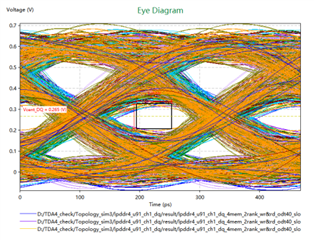
     We simulated LPDDR4 in IBIS model's slow mode, but failed at 4266 data rate(as it show as below), could you help review our board file cut in sigrity and give us some  advice (please contact xingyu-zhu@ti.com to get .spd file) ?
    Also we would liketo know, have you tried to simulate LPDDR4 signals in slow mode in the file "Jacinto 7 LPDDR4 Board Design and Layout Guidelines"?

     Looking foward to your reply as soon as possible. This question delay our gerber out time

  • Here is the spd file.

    https://e2e.ti.com/cfs-file/__key/communityserver-discussions-components-files/791/TDA4VMP_5F00_12L2_5F00_0925_5F00_cut.spd

  • Can the PCB design file be provided for review?  Sigrity (SPD) is a simulation file (my understanding).

  • Hi, sorry that we can not send you the PCB file to review it, but our layout are following the length matching rules, so the timing should be OK. The only thing we concern is the strength of buffer.
    We would like to know that have you passed the simulation in slow mode on your demo board?
    And under what circumstance should we consider the slow mode simulation?

  • The IBIS slow corner is: high temperature and low voltage.

    From the picture not clear if the eye is captured for a read or write simulation?

    Did you extract the PCB net impedances to verify their are no violations?

    Did you run multiple simulations to optimize ODI and ODT selection?  What values are you using?

    Did you follow our PCB recommendations for your design?

  • 1. this picture shows eyes captured from a set of dq signals of write simulation.
    2. the impedance of pcb net is controlled at 40ohm.
    3. the odi&odt are both set to 40ohm and this setting provides the biggest EYE diagram.
    4. we followed the lpddr4 board design and layout guidelines to design PCB and simulation settings, except for Routing Specifications"LP4_ACRS10": Center-to-center CK to other LPDDR4 trace spacing,  we use 3W instead of 4W. 

  • Agree the simulation results do not look good (fail mask requirements).  If the PCB guidelines are correctly followed, the simulation results should not look this bad.  Without additional information, it is difficult for TI to help identify areas of concern.  It is mentioned trace spacing could be an issue.  Can you confirm if the failures are a result of excessive crosstalk (due to trace spacing)? 

  • We tried to simulate a few signals to eliminate the crosstalk, and confirmed that crosstalk is not the main cause. It is the driving strength in slow mode too weak that cause the bad eye results. And we have already used the best odi&odt settings, but the rise time of these buffers in slow mode are too long.

    • How bad are the via stubs board?
    • What is the DQS impedance? Can you provide impedance plots of traces?
    • How did determine crosstalk is not the main issue?
      • Run a sim with just 1 bit active?
      • How does that eye compare to the eyes with all bits switching?
    • What is the variation in eye margin among the DQs? All are equally bad?
    • How good is the VSS reference plane?
    • Are all DDR signals referencing only the VSS plane? Any power plane referencing? Any return path discontinuities?
    • From the eye diagram caption snapshot  it seems using a quad die DRAM (2 rank). If so, how are setting the write ODT? One rank should have ODT and the other no ODT due to active and inactive ranks.
    • What is the p-p DDR PDN noise (at SOC pad and at DRAM pad) in sims?