This thread has been locked.

If you have a related question, please click the "Ask a related question" button in the top right corner. The newly created question will be automatically linked to this question.

AM4376: PRCM register setting

Guru 10105 points
Part Number: AM4376
Other Parts Discussed in Thread: TMDSEVM437X

Hi Support Team,

Our customer, who uses AM4376, has a question about register settings.

Question 1
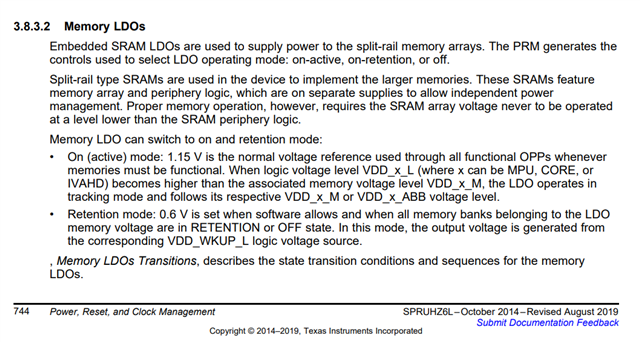
There is an expression "SRAMNWA" for the following register listed in TRM (www.ti.com/.../spruhl7i.pdf).
What does "SRAMNWA" mean?

PRCM_PRM_LDO_SRAM_CORE_SETUP
PRCM_PRM_LDO_SRAM_MPU_SETUP

Also, SRAMNWA supplied VDDS or VDDA can be selected by b[1] of PRCM_PRM_LDO_SRAM_CORE_SETUP register,
but what is the difference between VDDS and VDDAR?


Question 2
Regarding the PRCM_CM_WKUP_CLKDIV32K_CLKCTRL register
The optional functional clock can be enabled/disabled with b[8], but which function is affected by this register?
The register name is WKUP, but will it be a function setting related to Wake up?

I thought that CLKDIV32K might refer to CLK_32KHZ (32.768kHz) generated by the Peripheral PLL.
If this understanding is correct, though, CLK_32KHZ is routed to be used as the CLK for the Watchdog Timer (WDT),
In that case, is it necessary to enable the b[8] Optional functional clock in PRCM_CM_WKUP_CLKDIV32K_CLKCTRL?

Currently, the WDT seems to be working even with the b[8] Optional functional clock
in PRCM_CM_WKUP_CLKDIV32K_CLKCTRL set to disable.

Best Regards,
Kanae

  • Hello Kanae,

    Thank you for the query.

    Let me review the query and check internally on the right expert who would support the query.

    Please expect delay in response.

    Regards,

    Sreenivasa

  • Hi Sreenivasa,

    Thank you for your reply.
    If it takes a little longer to respond, please let me know when the right expert will be assigned
    and when a response will be available, so that I need to inform my customer.

    Best Regards,
    Kanae

  • Hello Kanae,

    Thank you for the note and understand.

    I will update you on the timeline in the next couple of days or answer i receive from the team.

    Regards,

    Sreenivasa

  • Hello Kanae,

    I looked into the AM335x, AM437x and AM572X and found the below description.

    I guess the SRAMNWA is SRAM network array.

    AM335x

    AM572x

    Regards,

    Sreenivasa

  • Hi Sreenivasa,

    Thanks for your support!

    The TRM of AM437x also clearly states the following.

    If SRAMNWA is an SRAM network array as you pointed out, does it mean that SRAMNWA specifically refers to the "Memory bank" in the above figure?

    In that case, when bit 1 of PRCM_PRM_LDO_SRAM_CORE_SETUP register: abboff_act_export is set to "1", SRAMNWA is supplied from VDDAR,
    but does "varray" in the above figure mean "VDDAR"?
    I do not understand it well, so please explain in detail.

    Also, if you could please explain the part clearly in the document for AM437x,
    it will be easier to explain to our customers.

    Please continue to help us with other questions as well.

    Best Regards,
    Kanae

  • Hello Kanae,

    Thank you for the inputs.

    If SRAMNWA is an SRAM network array as you pointed out, does it mean that SRAMNWA specifically refers to the "Memory bank" in the above figure?

    Please note that i am interpreting the datasheet (additionally referring AM335x and AM572x) to answer and based on the description i believe this is the memory section.

    In that case, when bit 1 of PRCM_PRM_LDO_SRAM_CORE_SETUP register: abboff_act_export is set to "1", SRAMNWA is supplied from VDDAR,
    but does "varray" in the above figure mean "VDDAR"?
    I do not understand it well, so please explain in detail.

    I assume VDDS is the external 1.8V input and VDDAR is the SRM LDO output. I guess Varray is the selected output and could be VDDS or VDDAR.

    Please refer AM437x datasheet 

    We can continue discussing Q1 in the thread.

    Q.2 To minimize any delay caused due to multiple topics included in the same thread, would you mind starting a new thread for me to assign to the right expert as we discuss Q1 in this thread.

    Regards,

    Sreenivasa

  • Hi Sreenivasa,

    Thank you for your detailed explanation.

    To summarize the answer to Q1,
    SRAMNWA" is the memory section in Figure 6-4.
    In the case of PRCM_PRM_LDO_SRAM_MPU_SETUP Register,
    VDDS is VDDS(2): Supply voltage range for all dual-voltage IO domains
    VDDAR : VDDS_SRAM_MPU_BB : Supply voltage range for MPU SRAM LDOs, Analog

    I will report your comments above to my customer, 
    and continue to post any additional questions in this thread.

    As for Q.2, I have started a new thread.

    https://e2e.ti.com/support/processors-group/processors/f/processors-forum/1277930/am4376-prcm_cm_wkup_clkdiv32k_clkctrl-register

    Best Regards,
    Kanae

  • Hello Kanae, 

    Thank you for understanding.

    Thank you for the note. Pls let me know when you hear from the customer.

    Regards,

    Sreenivasa

  • Hi Sreenivasa,

    The customer has an additional question and would appreciate your support.

    *****
    I understand that the PRCM_PRM_LDO_SRAM_MPU_SETUP register selects (VDDA or VDDAR)
    the power supply to the SRAM network array of the MPU.
    Could you please explain a little more about the relationship between VDDS, VDDAR, SRAMNWA,
    and the internal LDO for the SRAM?
    The datasheet "5.11.1.2 IO and Analog Voltage Decoupling Capacitors" states that
    VDDS_SRAM_CORE_BG supplies power to the internal LDO for SRAM.

    In addition, "5.11.2 Output Capacitors" shows a block diagram of the internal LDOs as follows.


    Based on the above, is the understanding of the power supply to SRAMNWA correct as follows?
    Also, are the voltages used by SRAMNWA different for VDDS and VDDAR?


    For PRCM_PRM_LDO_SRAM_MPU_SETUP register,

    VDDS: The power supplied to the VDDS pin from the outside is directly used for SRAMNWA
    *Is the voltage 1.8V used as it is? Or is VDDS also stepped down by internal LDO?

    VDDAR: Use the external power supply to the VDDS_SRAM_MPU_BB pin for SRAMNWA
    via the internal LDO.
    *Is the voltage stepped down to some V to solve the LDO?

    The power supply to the VDDS and VDDS_SRAM_MPU_BB pins of the CPU
    on the evaluation board is as follows, and we recognize that the power supplies for VDDS and VDDS_SRAM_MPU_BB are generated from the same source, 
    but the difference is whether or not a filter is used.
    *The current development model has the same connection configuration as the evaluation board.

    ******

    Best Regards,
    Kanae

  • Hello Kanae,

    Thank you.

    Please point me to the EVM you are referring.

    Regards,

    Sreenivasa

  • Hi Sreenivasa,

    Thank you for your support.

    My customer refer to TMDSEVM437X.

    https://www.ti.com/tool/ja-jp/TMDSEVM437X#design-files

    Best Regards,
    Kanae

  • Hello Kanae,

    Thank you.

    Let me review and come back.

    I am not able to find much information regarding VDDAR and checking internally.

    I am guessing this is some internal voltage.

    Please expect some delay. 

    Does customer have access to low-level power management control drivers for him to check the VDDAR related implementations.

    Pls help me understand the development environment customer is using.


    Regards,

    Sreenivasa

  • Hi Sreenivasa,

    Thank you for your support.

    Here are my customer's comments to your questions.


    Sreenivasa said;
    Does customer have access to low-level power management control drivers
    for him to check the VDDAR related implementations.

    What exactly do you mean by low-level power management control drivers?
    For example, the values of PRCM_PRM_DEVICE Registers that might be relevant to SRAM are

    PRCM_PRM_RSTCTRL (0x44df4000) = 0x00000000
    PRCM_PRM_RSTST (0x44df4004) = 0x00000001
    PRCM_PRM_RSTTIME (0x44df4008) = 0x0000004006
    PRCM_PRM_SRAM_COUNT (0x44df400c) = 0x78000017
    PRCM_PRM_LDO_SRAM_CORE_SETUP (0x44df4010) = 0x00000003
    PRCM_PRM_LDO_SRAM_CORE_CTRL (0x44df4014) = 0x00000000
    PRCM_PRM_LDO_SRAM_MPU_SETUP (0x44df4018) = 0x00000003
    PRCM_PRM_LDO_SRAM_MPU_CTRL (0x44df401c) = 0x00000000
    PRCM_PRM_IO_COUNT (0x44df4020) = 0x0000003A
    PRCM_PRM_IO_PMCTRL (0x44df4024) = 0x00010020
    PRCM_PRM_VC_VAL_BYPASS (0x44df4028) = 0x00000000

    Sreenivasa said;
    Pls help me understand the development environment customer is using.

    We are running TI SDK 7.3.0.5 Linux version on a custom board developed in-house.


    Please let me know if you have any other questions to check.

    Best Regards,
    Kanae

  • Hello Kanae,

    Thank you.

    What exactly do you mean by low-level power management control drivers?

    The ask was for customer to review if VDDS or VDDAR is being configured in the software and if these setting are being changed when the application is running to understand the use case and configuration.

    Refer below some observations based on the values customer provided.

    PRCM_PRM_LDO_SRAM_CORE_SETUP (0x44df4010) = 0x00000003

    PRCM_PRM_LDO_SRAM_CORE_CTRL (0x44df4014) = 0x00000000

    Regards,

    Sreenivasa


  • Hi Sreenivasa,

    Thank you for your support.
    My customer commented as follows, please continue to answer with the information you are confirming.

    I understand that the register setting means that the SRAMNWA supply in active mode is set to VDDAR
    from B[1] ABBOFF_ACT_EXPORT=1.
    PRCM_PRM_LDO_SRAM_CORE_SETUP (0x44df4010) = 0x00000003

    PRCM_PRM_LDO_SRAM_CORE_CTRL (0x44df4014) = 0x00000000
    I think this register is set with SRAMLDO enabled from B[8] SRAMLDO_STS=0.

    In other words, I understand that the SRAMNWA is currently powered via the internal LDO
    from the power supply connected to the VDDAR.

    What I would like to know is how the register settings related to VDDS, VDDAR,
    and internal LDO should be selected.
    You have posted that you will review the question as follows,
    and I would like to ask if this information you are reviewing may lead to the above understanding.

    ****
    Let me review and come back.
    I am not able to find much information regarding VDDAR and checking internally.
    I am guessing this is some internal voltage.
    *****

    Best Regards,
    Kanae

  • Hello Kanae,

    Thank you.

    Please search for VSLDO in the TRM.

    Refer below input i received from the expert:

    I don’t think you would need to change it from the efuse value except for debug.

    I guess i may not have any additional inputs.

    Regards,

    Sreenivasa

  • Hi Sreenivasa,
    Thank you for your support!

    Please let me confirm two points.
    1. Each LDO Integration figure could not be found in TRM.
    Which document did you refer to?

    2. Regarding the expert's opinion,
    "I don’t think you would need to change it from the efuse value except for debug."
    Is it your view that my customer should understand that there is no need to (or cannot)
    change the value of efuse, because no further response from the expert is expected?

    Best Regards,
    Kanae

  • Hello Kanae,

    Thank you.

    1. Each LDO Integration figure could not be found in TRM.
    Which document did you refer to?

    We do not have this in the TRM. This is the integration document.

    2. Regarding the expert's opinion,
    "I don’t think you would need to change it from the efuse value except for debug."
    Is it your view that my customer should understand that there is no need to (or cannot)
    change the value of efuse, because no further response from the expert is expected?

    Agree.

    Regards,

    Sreenivasa

  • Hi Sreenivasa,

    Thank you for your reply!
    I understand that the above figures are provided from an unpublished TI internal integration document.
    I would like to explain the above details to my customers so that he understands what you have shared with us.
    I would appreciate your support for any additional questions or inquiries.

    Best Regards,
    Kanae

  • Hello Kanae,

    Thank you.

    Regards,

    Sreenivasa

  • Hi Sreenivasa,

    Again, I am sorry, but please allow me to confirm the following items.

    Is it correct to understand that the voltage used to supply power to SRAMNWA differs between VDDS and VDDAR as shown in the figure below, and that when VDDAR is selected for SRAMNWA, the voltage is stepped down by the internal LDO?

    Or, if VDDS is selected, is it also stepped down by the internal LDO?

    Regarding eFuse, I have received a comment from your expert that it is not necessary
    to change from the efuse value except for debugging,
    Please let me confirm which part he is referring to.

    Best Regards,
    Kanae

  • Hello Kanae,

    Thank you.

    Regarding eFuse, I have received a comment from your expert that it is not necessary
    to change from the efuse value except for debugging,
    Please let me confirm which part he is referring to.

    The default register values are programmed into the registers using internal memory and this is the eFuse. This is not external.

    When changes are required, during power-up the eFuse (default configuration) is read and then the software makes the required configuration. 

     Regards,

    Sreenivasa

  • Hello Kanae,

    For the VDDAR there are trim registers and so i guess the input is being regulated 

    Is it correct to understand that the voltage used to supply power to SRAMNWA differs between VDDS and VDDAR as shown in the figure below, and that when VDDAR is selected for SRAMNWA, the voltage is stepped down by the internal LDO?

    Regarding the VDDS i guess this is using the external 1.8V applied.

    Regards,

    Sreenivasa

  • Hi Sreenivasa,

    Thank you for your support!

    My customer does not want to change the default register values,
    so I don't think it is a problem.

    I appreciate your clarification of the following customer concerns.
    - VDDAR has a trim register, so the input is adjusted.
    - As for VDDS, it uses an external 1.8V.

    Best Regards,
    Kanae

  • Hello Kanae,

    Thank you for the note.

    I am closing the thread.

    Regards,

    Sreenivasa