This thread has been locked.

If you have a related question, please click the "Ask a related question" button in the top right corner. The newly created question will be automatically linked to this question.

AM6442: About access priority to DDR.

Part Number: AM6442
Other Parts Discussed in Thread: SYSCONFIG

I changed the DDR access priority using "Class of Service (CoS)" of DDRSS and confirmed the operation of DDR access.
However, the results were not as expected.

What I confirmed are the following (a) and (b).

(a):
  Leave the "Class of Service" as default (all with the same priority), continue to write 4 Bytes to DDR with the R5F core, and obtain the time it takes for the A53 core to read 4 Bytes to DDR while R5F is writing.
  If you increase the number of R5F cores that perform 4Byte Writes to DDR, the time it takes for A53 cores to read 4Bytes to DDR will also increase.
  This is the expected result.

(b):
  In "Class of Service", change the priority of the A53 core to high and the other priorities to low, and check the same as in (a).
  Since I changed the DDR access priority of the A53 core to high, I thought that the time required for reading the A53 core would be shorter than in (a), but the result is the same as in (a).

Please let me know about my next question.
Q1:
  Why is the result in (b) the same as in (a)?

Q2:
  Am I using DDRSS's "Class of Service (CoS)" incorrectly?

I have attached the project used for confirmation.

For information on configuring Class of Service, refer to the next chapter of TRM.
  AM64x/AM243x Technical Reference Manual (Rev. G)
    3.3.1 Route ID
    8.1.4.1 Class of Service (CoS)


I'm using the following environment:
  AM64x EVM TMDS64GPEVM (SR1.0)
  AM64x MCU+ SDK (Ver.08.03.00)
    Example:Empty Project
 Code Composer Studio (Ver.12.4.0)
 SysConfig Tool (Ver.1.12.1)

DDRSS_CoS.zip

  • There might be a few reasons for the behavior you are seeing:

    -are you running with cache enabled?  The data may already be cached and thus the access to the data doesn't need to go all the way out to the memory

    -i'm not sure what you are using to time your accesses.  Maybe there is not enough granularity in the timer to perceive a difference with just 4 bytes

    -the DDR controller could be reordering the commands to optimize accesses  

    -Not sure how you coding the accesses to the DDR.  It will make a difference if you are using single cycle accesses, loops, different element sizes, DMAs, etc.

    Regards,

    James

  • Hello James,
    Thank you for your reply.

    -are you running with cache enabled? The data may already be cached and thus the access to the data doesn't need to go all the way out to the memory
    Cache is enabled, but I set the DDR area that performs memory access to non-cache with MMU/MPU.

    -i'm not sure what you are using to time your accesses. Maybe there is not enough granularity in the timer to perceive a difference with just 4 bytes
    I am using a Performance Monitor Unit (PMU) cycle counter.

    -the DDR controller could be reordering the commands to optimize accesses
    Is the order changed even when memory accesses are made to the same address?

    -Not sure how you coding the accesses to the DDR. It will make a difference if you are using single cycle accesses, loops, different element sizes, DMAs, etc.
    R5F core:
      Loop 4Bytes write (STR instruction 100 times) to the same address
    A53 core:
      Loop 4Bytes read (LDR instruction once) to the address being written by the R5F core (256 times).
      In the loop, we read the PMU's cycle counter and check the average time it takes to read the DDR.

    I have attached the CCS project to my first post, so please see "empty.c" for details.

    Regards.

  • Greetings Tomitama,

    The DDR Class of Service feature does allow accesses to have different priorities, but ultimately the DDR controller will re-order them based on the state of the DRAM (like which banks are currently open so it doesn't incur an extra miss). This means that even though one access may have a higher priority, a lower priority command may execute before it. This is one of the key features of the DDR controller to make optimal use of the DDR DRAM when there are many accesses at once.

    Sincerely,

    Lucas

  • DDR CoS is intended to prioritize some initiator over others. So there needs to be interfering traffic from some other initiator to see an effect. The A53 is designed to operate for high memory throughput through cached memory, specifically the shared L2 cache, not for non-cached to DDR from each individual core. The non-cached access from A53 to DDR is not performance optimized in the A53 core, the CoS should be set for the cluster (L2 cache) and the benchmark to use would be some throughput or bandwidth oriented one. 

    What route ID are you using for the A53? I noticed it is not that clear in the TRM, but 0 and 1 should be the non-cacheable strongly ordered access from each of the 2 cores. 4 is the shared L2 cache. For any normal SW only the shared cache should matter.

    R5F core:
      Loop 4Bytes write (STR instruction 100 times) to the same address
    A53 core:
      Loop 4Bytes read (LDR instruction once) to the address being written by the R5F core (256 times).
      In the loop, we read the PMU's cycle counter and check the average time it takes to read the DDR.

    I'm not clear what this is intended to measure. The sequence is shared memory, so coherency related features will come into play in the DDR controller. CoS is intended for relative prioritization of independent access streams. R5 working on memory at one address, A53 at another. CoS can be used to improve one of these over the other. Depending on what is the intention I would think R5 and A53 should work on completely different DDR locations to see relative priority.

    As a summary CoS is a tool to say no matter what this other core or DMA is doing, I want to to prioritize this core.

  • I am using 0 and 16 as Route IDs for A53, which are IDs corresponding to COMPUTE_CLUSTER0 described in TRM (Rev.G).
    Please let me know what is not clear in RouteID's TRM.

    My aim is to check about two things:
      1.DDR CoS priority change has given priority to A53 core over R5 core.
      2.Difference in processing time required when DDR CoS priority is changed and when the priority is the same.
    Please let me know if there are any specific steps to confirm the above.

    I changed the memory access address to a different address for each core, but I could not see any difference due to the DDR CoS priority change.
    Using the following DDR address:
      A53:0x86000000
      R5_0_0:0x90000000
      R5_0_1:0xA0000000
      R5_1_0:0xB0000000
      R5_1_1:0xC0000000

  • Greetings Tomitama,

      1.DDR CoS priority change has given priority to A53 core over R5 core.
      2.Difference in processing time required when DDR CoS priority is changed and when the priority is the same.

    Understand you're looking to verify features, but can you elaborate on what are your goal(s) for using CoS? Are you trying to accelerate some application or ensure some kind of time deadline? This will help us understand and possibly suggest other ideas for your overall goal(s). 

    Pekka is correct as stated above, the practical usecase for the cores is for high throughput applications that have DDR set as cacheable (in the MMU for A53 and MPU for R5) so that it will send cacheline fetches (64B for A53, 32B for R5) to DDR. 

    When a lot of high throughput initiators (core/DMA/other) saturate the bandwidth of the DDR at once this could create starvation on some of their threads, as a result they could see severely lowered throughput. CoS is one mechanism to mitigate that, but may not show a noticeable difference unless there is a high amount of traffic. The available bandwidth of DDR is dependent on the speed of it's operation (16-bit DDR at 1600MT/s is a bit lower that 3200MB/s) so you may not even come close to using up available bandwidth for your overall usecase (DDR speed, IPs being used, access pattern, etc.) 

    Sincerely,

    Lucas

  • From the A53 the standard C-library memcpy() (or memset()) will utilize optimized memory access instructions that with be able to generate almost 70% of the theoretical wire rate at the DDR interface. From Linux this gets called with for example bw_mem -P 2 8M bcopy this will generate maximum number of outstanding cache line operations from the 2 A53s at the memory controller. This will be much higher load than the inline assembly that I can see in the attached project. Without a flood of interfering memory reads/writes you will not see any difference in access latency. Similar with R5. Would suggest to modify the background load to be a memset() or memcpy(), measure typical latency from the other core while the interfering core is doing memset() or memcpy().

  • I'm expecting the following behavior by changing the CoS priority:
      For example, if there are three cores with the same priority and they access the same memory address, the access time will be about the same.
      If only one core has a high priority and three cores access the same memory address, the access time of the core with a high priority will be faster.

    In other words, I expect that the higher priority core's access will be prioritized when accessing the same memory address.

    Can the above behavior be achieved by using CoS?

    The above sequence makes sense for non-cached SRAM, but not for cached LPDDR4/DDR4. LPDDR4 CoS is meant for average bandwidth and average latency of accesses in an oversubscribed case. There are a few underlying reasons for this, I'm listing some of them here:

    - LPDDR4 on AM64x has a base read latency in the ballpark of 200ns, so about 200 clock cycles from A53. One non-cached read means stall for ~199 cycles
    - Only cached accesses make sense to LPDDR4, otherwise performance is bad
    - LPDDR4 works with bursts, each read consumes 16 beats of 16-bit wide, so 32bytes come every ready even if you ask for 1 byte, reading one byte/word is really inefficient
    - Put the above together, only cached accesses make sense for anything performance oriented
    - The CoS works with the command queue of 32 commands, picking the command based on a number of factors one but not the only one of which is CoS

    So to tests CoS I would suggest have high priority read from a core. Measure the latency of that read in an otherwise idle system. In our Linux performance guide lat_mem_rd is the microbenchmark. To see the effect of interfering traffic run memcpy() to some LPDDR4 address from an interfering core. Change to CoS of that core to be above or below the high priority core.

    Uncached single reads from R5 or A53 will not be able to saturate the LPDDR4 controller, so most likely CoS settings have no effect on observed read latencies.

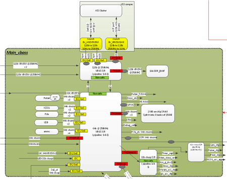
  • Adding a further detail here. The TRM does not have the detailed topology, instead just a simplified "CBASS0" for all of the interconnect. This is the more exact way the interconnect is done, A53 to LPDDR4/DDR4 on one block, then the rest of the main initiators on another.