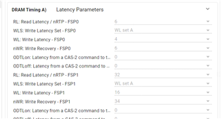
1.I know DRAM timing A ,the most part of them is auto calculated.
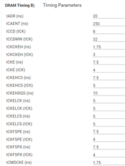
2.DRAM timing B,I understand these parameters is coming from datasheet.But someone of them can not find.
such as tCKFSPE,tCKFSPX.
3.IOControl A IOCONTROLB,does it coming from DDR datasheet also?
But I can find some parameters also.
such as:
| VREF Control Range Lane 0/1 DQ/DM/DQS |
what does range0 stand for?

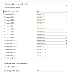
4 Bit Swizzle / Byte Swap for Bytes 0/1.I suppose it is related data MSB or LSB? Am I right?
And for SDK 9.0,whether the configuration as follow is proper?