This thread has been locked.

If you have a related question, please click the "Ask a related question" button in the top right corner. The newly created question will be automatically linked to this question.

TDA4VL-Q1: TDA4VL boot from ospi fail

Part Number: TDA4VL-Q1
Other Parts Discussed in Thread: TDA4VL

Hi, experts ,

I am debugging tda4vl(sdk 0806) to boot from ospi and the following prompt error appears:

SPL: failed to boot from all boot devices
### ERROR ### Please RESET the board ###

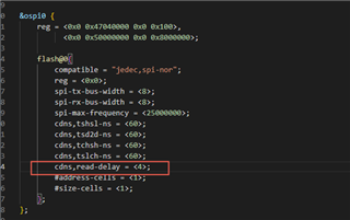
I copied tiboot3. bin, tispl. bin, and u boot. img from Linux to OSPI flash, and the results read from OPSI flash are consistent with the source file.

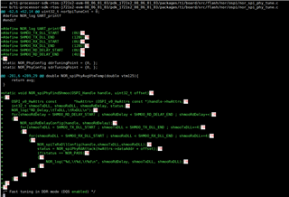
I added printing information to the ti-processor-sdk-linux-j721s2-evm-08_06_01_02/board-support/u-boot-2021.01+gitAUTOINC+62a9e51344-g62a9e51344/common/spl/spl_spi.c  file and found that the  spl_parse_image_header function returned an error value,

Please help me analyze this issue,thanks!

Best Regards,

Bing

  • // SPDX-License-Identifier: GPL-2.0+
    /*
     * Copyright (C) 2011 OMICRON electronics GmbH
     *
     * based on drivers/mtd/nand/raw/nand_spl_load.c
     *
     * Copyright (C) 2011
     * Heiko Schocher, DENX Software Engineering, hs@denx.de.
     */
    
    #include <common.h>
    #include <image.h>
    #include <log.h>
    #include <spi.h>
    #include <spi_flash.h>
    #include <errno.h>
    #include <spl.h>
    
    DECLARE_GLOBAL_DATA_PTR;
    
    #ifdef CONFIG_SPL_OS_BOOT
    /*
     * Load the kernel, check for a valid header we can parse, and if found load
     * the kernel and then device tree.
     */
    static int spi_load_image_os(struct spl_image_info *spl_image,
    			     struct spi_flash *flash,
    			     struct image_header *header)
    {
    	int err;
    
    	/* Read for a header, parse or error out. */
    	spi_flash_read(flash, CONFIG_SYS_SPI_KERNEL_OFFS, sizeof(*header),
    		       (void *)header);
    
    	if (image_get_magic(header) != IH_MAGIC)
    		return -1;
    
    	err = spl_parse_image_header(spl_image, header);
    	if (err)
    		return err;
    
    	spi_flash_read(flash, CONFIG_SYS_SPI_KERNEL_OFFS,
    		       spl_image->size, (void *)spl_image->load_addr);
    
    	/* Read device tree. */
    	spi_flash_read(flash, CONFIG_SYS_SPI_ARGS_OFFS,
    		       CONFIG_SYS_SPI_ARGS_SIZE,
    		       (void *)CONFIG_SYS_SPL_ARGS_ADDR);
    
    	return 0;
    }
    #endif
    
    static ulong spl_spi_fit_read(struct spl_load_info *load, ulong sector,
    			      ulong count, void *buf)
    {
    	struct spi_flash *flash = load->dev;
    	ulong ret;
    
    	ret = spi_flash_read(flash, sector, count, buf);
    	if (!ret)
    		return count;
    	else
    		return 0;
    }
    
    unsigned int __weak spl_spi_get_uboot_offs(struct spi_flash *flash)
    {
    	return CONFIG_SYS_SPI_U_BOOT_OFFS;
    }
    
    u32 __weak spl_spi_boot_bus(void)
    {
    	return CONFIG_SF_DEFAULT_BUS;
    }
    
    u32 __weak spl_spi_boot_cs(void)
    {
    	return CONFIG_SF_DEFAULT_CS;
    }
    
    /*
     * The main entry for SPI booting. It's necessary that SDRAM is already
     * configured and available since this code loads the main U-Boot image
     * from SPI into SDRAM and starts it from there.
     */
    static int spl_spi_load_image(struct spl_image_info *spl_image,
    			      struct spl_boot_device *bootdev)
    {
    	int err = 0;
    	unsigned int payload_offs;
    	struct spi_flash *flash;
    	struct image_header *header;
    	unsigned int sf_bus = spl_spi_boot_bus();
    	unsigned int sf_cs = spl_spi_boot_cs();
    
    	/*
    	 * Load U-Boot image from SPI flash into RAM
    	 * In DM mode: defaults speed and mode will be
    	 * taken from DT when available
    	 */
    	flash = spi_flash_probe(sf_bus, sf_cs,
    				CONFIG_SF_DEFAULT_SPEED,
    				CONFIG_SF_DEFAULT_MODE);
    	if (!flash) {
    		puts("SPI probe failed.\n");
    		return -ENODEV;
    	}
    
    	payload_offs = spl_spi_get_uboot_offs(flash);
    
    	header = spl_get_load_buffer(-sizeof(*header), sizeof(*header));
    
    #if CONFIG_IS_ENABLED(OF_CONTROL) && !CONFIG_IS_ENABLED(OF_PLATDATA)
    	payload_offs = fdtdec_get_config_int(gd->fdt_blob,
    					     "u-boot,spl-payload-offset",
    					     payload_offs);
    #endif
    	printf("[%s: %d] ******** payload_offs = %u\n", __func__, __LINE__, payload_offs);
    #ifdef CONFIG_SPL_OS_BOOT
    	if (spl_start_uboot() || spi_load_image_os(spl_image, flash, header))
    #endif
    	{
    		/* Load u-boot, mkimage header is 64 bytes. */
    		err = spi_flash_read(flash, payload_offs, sizeof(*header),
    				     (void *)header);
    		printf("[%s: %d] ******** err = %u\n", __func__, __LINE__, err);
    		if (err) {
    			printf("%s: Failed to read from SPI flash (err=%d)\n",
    			      __func__, err);
    			return err;
    		}
    		printf("[%s: %d] ******** err = %u\n", __func__, __LINE__, err);
    		if (IS_ENABLED(CONFIG_SPL_LOAD_FIT_FULL) &&
    		    image_get_magic(header) == FDT_MAGIC) {
    			err = spi_flash_read(flash, payload_offs,
    					     roundup(fdt_totalsize(header), 4),
    					     (void *)CONFIG_SYS_LOAD_ADDR);
    			printf("[%s: %d] ******** err = %u\n", __func__, __LINE__, err);
    			if (err)
    				return err;
    			printf("[%s: %d] ******** err = %u\n", __func__, __LINE__, err);
    			err = spl_parse_image_header(spl_image,
    					(struct image_header *)CONFIG_SYS_LOAD_ADDR);
    		} else if (IS_ENABLED(CONFIG_SPL_LOAD_FIT) &&
    			   image_get_magic(header) == FDT_MAGIC) {
    			struct spl_load_info load;
    			printf("[%s: %d] ******** err = %u\n", __func__, __LINE__, err);
    			printf("Found FIT\n");
    			load.dev = flash;
    			load.priv = NULL;
    			load.filename = NULL;
    			load.bl_len = 1;
    			load.read = spl_spi_fit_read;
    			err = spl_load_simple_fit(spl_image, &load,
    						  payload_offs,
    						  header);
    		} else if (IS_ENABLED(CONFIG_SPL_LOAD_IMX_CONTAINER)) {
    			struct spl_load_info load;
    			printf("[%s: %d] ******** err = %u\n", __func__, __LINE__, err);
    			load.dev = flash;
    			load.priv = NULL;
    			load.filename = NULL;
    			load.bl_len = 1;
    			load.read = spl_spi_fit_read;
    
    			err = spl_load_imx_container(spl_image, &load,
    						     payload_offs);
    		} else {
    			printf("[%s: %d] ******** err = %u\n", __func__, __LINE__, err);
    			err = spl_parse_image_header(spl_image, header);
    			printf("[%s: %d] ******** err = %u\n", __func__, __LINE__, err);
    			if (err)
    				return err;
    			printf("[%s: %d] ******** err = %u\n", __func__, __LINE__, err);
    			err = spi_flash_read(flash, payload_offs,
    					     spl_image->size,
    					     (void *)spl_image->load_addr);
    		}
    		printf("[%s: %d] ******** err = %u\n", __func__, __LINE__, err);
    		if (IS_ENABLED(CONFIG_SPI_FLASH_SOFT_RESET)) {
    			printf("[%s: %d] ******** err = %u\n", __func__, __LINE__, err);
    			err = spi_nor_remove(flash);
    			if (err)
    				return err;
    			printf("[%s: %d] ******** err = %u\n", __func__, __LINE__, err);
    		}
    	}
    
    	return err;
    }
    /* Use priorty 1 so that boards can override this */
    SPL_LOAD_IMAGE_METHOD("SPI", 1, BOOT_DEVICE_SPI, spl_spi_load_image);
    

    spl_spi.c

  • Thanks for posting your question to TI processor's E2E forum. The expert assigned to this thread is out of office due to public holidays in India today. Please expect a response by the end of this week.

  • Hi,

    Is this a custom board? If yes which flash part is being used?

    Regards,

    Keerthy

  • Yes, we are using custom boards.The datasheet for flash is as followsGD25LX256EB2RR .pdf

  • ospi flash partition info:

    root@j721s2-evm:/ospi# cat /proc/mtd
    dev:    size   erasesize  name
    mtd0: 00080000 00010000 "ospi.tiboot3"
    mtd1: 00200000 00010000 "ospi.tispl"
    mtd2: 00400000 00010000 "ospi.u-boot"
    mtd3: 00040000 00010000 "ospi.env"
    mtd4: 00040000 00010000 "ospi.env.backup"
    mtd5: 01600000 00010000 "ospi.rootfs"
    mtd6: 00010000 00010000 "ospi.phypattern"
    

    flashing boot files to ospi:

    root@j721s2-evm:/ospi# cat update.sh
    #!/bin/sh
    
    #mount /dev/mmcblk1p1 /tmp/
    
    
    dd if=/ospi/tiboot3.bin of=/dev/mtdblock0
    dd if=/ospi/tispl.bin of=/dev/mtdblock1
    dd if=/ospi/u-boot.img of=/dev/mtdblock2
    dd if=/ospi/nor_spi_patterns.bin of=/dev/mtdblock6
    
    root@j721s2-evm:/ospi# ./update.sh
    790+1 records in
    790+1 records out
    404730 bytes (405 kB, 395 KiB) copied, 17.0873 s, 23.7 kB/s
    1907+1 records in
    1907+1 records out
    976520 bytes (977 kB, 954 KiB) copied, 38.1969 s, 25.6 kB/s
    2154+1 records in
    2154+1 records out
    1103124 bytes (1.1 MB, 1.1 MiB) copied, 42.1821 s, 26.2 kB/s
    0+1 records in
    0+1 records out
    128 bytes copied, 1.47849 s, 0.1 kB/s
    

  • Hi,

    The tiboot3.bin is coming up and the next stages are not coming up. Can you share the addresses to which you are flashing the tispl.bin and U-Boot.img.?

    Also share the OSPI boot logs in a text file.

    Best Regards,

    Keerthy 

  • ospi boot log

    U-Boot SPL 2021.01 (Nov 07 2023 - 11:24:11 +0800)
    ti_sci system-controller@44083000: Message not acknowledgedti_sci system-controller@44083000: Message not acknowledgedSYSFW ABI: 3.1 (firmware rev 0x0008 '8.6.3--1-g2249f (Chill Capybara')
    SPL initial stack usage: 13472 bytes
    ++++++++++++++ spl_boot = 3
    ++++++++++++++ spl_boot = 3735928559
    ++++++++++++++ spl_boot = 3735928559
    ++++++++++++++ spl_boot = 3735928559
    ++++++++++++++ spl_boot = 3735928559
    Trying to boot from SPI
    [spl_load_image: 530] ********
    [spi_nor_scan: 3785] ********
    ******** JEDEC id bytes: c8, 68, 19
    [spi_nor_set_fixups: 3733] ********
    [spi_nor_micron_octal_dtr_enable: 3497] ******** change buf from 20 to 16
    [spi_nor_micron_octal_dtr_enable: 3511] ******** change read_dummy from 20 to 16
    [spl_spi_load_image: 134] ******** payload_offs = 0x80000
    Magic number: 0xedfe0d
    Image Header CRC Checksum: 0xa80500
    Size: 2360576 bytes
    Load address: 0x280000
    Entry point: 0x110000
    Image Data CRC Checksum: 0x100000
    OS type: 0
    Architecture: 0
    Image type: 0
    Compression type: 0
    Name:
    [spl_spi_load_image: 143] ******** Magic = 0xdfeed00
    [spl_spi_load_image: 144] ******** err = 0
    [spl_spi_load_image: 150] ******** err = 0
    [spl_spi_load_image: 188] ******** err = 0
    [spl_parse_image_header: 274] ********
    [spl_parse_image_header: 329] ********
    [spl_spi_load_image: 190] ******** err = -22
    [spl_load_image: 544] ******** ret = -22
    SPL: failed to boot from all boot devices
    ### ERROR ### Please RESET the board ###

    partitions info:

    [ 11.767165] spi-nor spi0.0: gd25lx256e (32768 Kbytes)
    [ 11.830358] 7 cmdlinepart partitions found on MTD device 47040000.spi.0
    [ 11.912883] Creating 7 MTD partitions on "47040000.spi.0":
    [ 11.981310] 0x000000000000-0x000000080000 : "ospi.tiboot3"
    [ 12.058407] 0x000000080000-0x000000280000 : "ospi.tispl"
    [ 12.130571] 0x000000280000-0x000000680000 : "ospi.u-boot"
    [ 12.203821] 0x000000680000-0x0000006c0000 : "ospi.env"
    [ 12.273660] 0x0000006c0000-0x000000700000 : "ospi.env.backup"
    [ 12.351104] 0x000000800000-0x000001e00000 : "ospi.rootfs"
    [ 12.424156] 0x000001ff0000-0x000002000000 : "ospi.phypattern"

  • I found out there was an error reading the magic number

    ti-processor-sdk-linux-j721s2-evm-08_06_01_02/board-support/u-boot-2021.01+gitAUTOINC+62a9e51344-g62a9e51344/common/spl/spl_spi.c

    spl_spi_load_image -> 
                                      else if (IS_ENABLED(CONFIG_SPL_LOAD_FIT) &&
                                              image_get_magic(header) == FDT_MAGIC) { 
                   
  • There were no mistakes when I was flashing,because I made the following modifications and it was successful

    spi-tx-bus-width = <8>; -->  spi-tx-bus-width = <1>;
    spi-rx-bus-width = <8>; --> spi-rx-bus-width = <1>;
  • Hi Bing,

    https://software-dl.ti.com/jacinto7/esd/processor-sdk-rtos-j721s2/09_00_01_01/exports/docs/psdk_rtos/docs/user_guide/evm_setup_j721s2.html#xspi-boot-mode

    J721s2 supports only xSPI mode. I believe you are already using the xSPI boot mode as you are seeing traces of R5 SPL. Can you confirm that?

    - Keerthy

  • I am using OSPI boot mode.

    "J721s2 supports only xSPI mode" --  I checked the TRM document and it supports ospI boot mode, So I chose the OSPI boot mode.

  • Hi Bing,

    Agreed the SOC is supporting but the U-Boot does not support the OSPI boot mode as xSPI is already supported.
    Can you please try xSPI?

    - Keerthy

  • "Can you please try xSPI?"

    I have tried, but there are still issues.

    What is ”cdns,read-delay “ used for configuration? I changed it to 1 and board can boot normally,configure SOC read data delay?
    How to configure this parameter in PDK? Because I also encountered a problem when boot using SBL method
  • Hi,

    I changed it to 1 and board can boot normally,configure SOC read data delay?

    That is good. So SPL is working. I will loop in our SBL expert for this.

    - Keerthy

  • Thank you. Looking forward to your reply

  • Hi,exports

    SBL log:

    ▒▒ ▒▒▒▒SBL Revision: 01.00.10.01 (Nov 9 2023 - 17:56:57)
    TIFS ver: 8.6.3--1-g2249f (Chill Capybara
    Initlialzing PLLs ...done.
    InitlialzingClocks ...done.
    Initlialzing DDR ...done.
    Initializing GTC ...Begin parsing user application
    OSPI RCLK running at 166666666 MHz.


    Fast Tuning at temperature -45C
    [Nor_spiPhyDdrTune: 304] rdDelay = 1
    Unable to find RX Min
    Ospi Read speed for 0x4 bytes from offset 0x280000 = 0 Mbytes per sec


    Fast Tuning at temperature 34C
    [Nor_spiPhyDdrTune: 304] rdDelay = 1
    Unable to find RX Min
    Ospi Read speed for 0x10 bytes from offset 0x280000 = 0 Mbytes per sec
    Invalid magic number in Single image header
    SBL_ospiClose called
    BootImage...FAILED

  • Hi,

    Looks like PHY tuning is failing. Can you please share more details? Which SDK version are you using and what are the changes that you have done to adapt to this flash in SDK?

    Regards,
    Parth

  • The SDK version we are using is 0806

    Add our flash to SDK and make the following specific changes:

    diff --git a/ti-processor-sdk-rtos-j721s2-evm-08_06_01_03/pdk_j721s2_08_06_01_03/packages/ti/board/src/flash/include/board_flash.h b/ti-processor-sdk-rtos-j721s2-evm-08_06_01_03/pdk_j721s2_08_06_01_03/packages/ti/board/src/flash/include/board_flash.h
    index ea6d011fcc..0a6cc364fe 100644
    --- a/ti-processor-sdk-rtos-j721s2-evm-08_06_01_03/pdk_j721s2_08_06_01_03/packages/ti/board/src/flash/include/board_flash.h
    +++ b/ti-processor-sdk-rtos-j721s2-evm-08_06_01_03/pdk_j721s2_08_06_01_03/packages/ti/board/src/flash/include/board_flash.h
    @@ -127,6 +127,7 @@ typedef int32_t Board_flash_STATUS;       /** Board Flash API return type */
     #define BOARD_FLASH_ID_MT28EW256ABA        (0x227EU)  /* Device Id code 1 */
     #define BOARD_FLASH_ID_CY7C10612G          (0)
     #define BOARD_FLASH_ID_W35N01JWTBAG        (0xDC21U) /**< Winbond 1GB NAND flash */
    +#define BOARD_FLASH_ID_GD25LX256E          (0x6819)  /** Giga device 256Mbit NOR Flash **/
     
     /**
      * @brief 	Board specific Flash Device Identifiers.
    diff --git a/ti-processor-sdk-rtos-j721s2-evm-08_06_01_03/pdk_j721s2_08_06_01_03/packages/ti/board/src/flash/nor/device/gd25lx256e.h b/ti-processor-sdk-rtos-j721s2-evm-08_06_01_03/pdk_j721s2_08_06_01_03/packages/ti/board/src/flash/nor/device/gd25lx256e.h
    new file mode 100644
    index 0000000000..0534db1a41
    --- /dev/null
    +++ b/ti-processor-sdk-rtos-j721s2-evm-08_06_01_03/pdk_j721s2_08_06_01_03/packages/ti/board/src/flash/nor/device/gd25lx256e.h
    @@ -0,0 +1,155 @@
    +/*
    + * Copyright (c) 2020, Texas Instruments Incorporated
    + * All rights reserved.
    + *
    + * Redistribution and use in source and binary forms, with or without
    + * modification, are permitted provided that the following conditions
    + * are met:
    + *
    + * *  Redistributions of source code must retain the above copyright
    + *    notice, this list of conditions and the following disclaimer.
    + *
    + * *  Redistributions in binary form must reproduce the above copyright
    + *    notice, this list of conditions and the following disclaimer in the
    + *    documentation and/or other materials provided with the distribution.
    + *
    + * *  Neither the name of Texas Instruments Incorporated nor the names of
    + *    its contributors may be used to endorse or promote products derived
    + *    from this software without specific prior written permission.
    + *
    + * THIS SOFTWARE IS PROVIDED BY THE COPYRIGHT HOLDERS AND CONTRIBUTORS "AS IS"
    + * AND ANY EXPRESS OR IMPLIED WARRANTIES, INCLUDING, BUT NOT LIMITED TO,
    + * THE IMPLIED WARRANTIES OF MERCHANTABILITY AND FITNESS FOR A PARTICULAR
    + * PURPOSE ARE DISCLAIMED. IN NO EVENT SHALL THE COPYRIGHT OWNER OR
    + * CONTRIBUTORS BE LIABLE FOR ANY DIRECT, INDIRECT, INCIDENTAL, SPECIAL,
    + * EXEMPLARY, OR CONSEQUENTIAL DAMAGES (INCLUDING, BUT NOT LIMITED TO,
    + * PROCUREMENT OF SUBSTITUTE GOODS OR SERVICES; LOSS OF USE, DATA, OR PROFITS;
    + * OR BUSINESS INTERRUPTION) HOWEVER CAUSED AND ON ANY THEORY OF LIABILITY,
    + * WHETHER IN CONTRACT, STRICT LIABILITY, OR TORT (INCLUDING NEGLIGENCE OR
    + * OTHERWISE) ARISING IN ANY WAY OUT OF THE USE OF THIS SOFTWARE,
    + * EVEN IF ADVISED OF THE POSSIBILITY OF SUCH DAMAGE.
    + *
    + */
    +
    +/**
    + *
    + * \file  s28hs512t.h
    + *
    + * \brief This file contains GD25LX256E NOR device definitions
    + *
    + *****************************************************************************/
    +#ifndef GD25LX256E_H_
    +#define GD25LX256E_H_
    +
    +#include <ti/drv/spi/SPI.h>
    +
    +#ifdef __cplusplus
    +extern "C" {
    +#endif
    +
    +/**************************************************************************
    + **                       Macro Definitions
    + **************************************************************************/
    +
    +/** FLASH device specific items (note: sizes are in bytes) */
    +#define NOR_BLOCK_SIZE               (256U * 1024U)
    +/* The Smallest Hybrid sector size is 4-KB */
    +#define NOR_SECTOR_SIZE              (4U * 1024U)
    +/* The Hybrid sector size of 64-KB */
    +#define NOR_HYBRID_SECTOR_SIZE       NOR_BLOCK_SIZE
    +#define NOR_SIZE                     (64U * 1024U * 1024U)
    +/** Physical set of thirty two 4-KB sectors at top or bottom of the address space */
    +#define NOR_NUM_4KSECTORS            (32U)
    +#define NOR_NUM_SECTORS              NOR_NUM_4KSECTORS
    +#define NOR_NUM_BLOCKS               (NOR_SIZE / NOR_BLOCK_SIZE)
    +#define NOR_PAGE_SIZE                (256U)
    +#define NOR_NUM_PAGES_PER_SECTOR     (NOR_SECTOR_SIZE / NOR_PAGE_SIZE)
    +#define NOR_NUM_PAGES_PER_BLOCK      (NOR_BLOCK_SIZE / NOR_PAGE_SIZE)
    +
    +#define NOR_4K_SECT_BOT_END_OFFSET   (0x1FFFF)
    +
    +/** Flash device commands */ 
    +#define NOR_BE_SECTOR_NUM            (-1U)
    +
    +#define NOR_CMD_BULK_ERASE           (0xC7U)
    +#define NOR_CMD_WRREG                (0x71U)
    +#define NOR_CMD_WREN                 (0x06U)
    +#define NOR_CMD_WRDIS                (0x04U)
    +#define NOR_CMD_RDSR                 (0x05U)
    +#define NOR_CMD_RDSR2                (0x07U)
    +#define NOR_CMD_RDREG                (0x65U)
    +#define NOR_CMD_RDCR                 (0x35U)
    +#define NOR_CMD_RDID                 (0x9FU)
    +#define NOR_CMD_SRSTE                (0x66U)
    +#define NOR_CMD_SFRST                (0x99U)
    +
    +#define NOR_CMD_BLOCK_ERASE          (0xDCU)
    +#define NOR_CMD_SECTOR_ERASE         (0x21U)
    +#define NOR_CMD_READ                 (0x03U)
    +#define NOR_CMD_FAST_READ            (0x0BU)
    +#define NOR_CMD_OCTAL_READ           (0xECU)
    +#define NOR_CMD_OCTAL_DDR_READ       (0xEEU)
    +#define NOR_CMD_PAGE_PROG            (0x02U)
    +#define NOR_CMD_OCTAL_PROG           (0x12U)
    +#define NOR_CMD_WRITE_VCR            (0x71U)
    +#define NOR_CMD_READ_VCR             (0x85U)
    +
    +#define NOR_VREG_OFFSET              (0x80U)
    +#define NOR_NVREG_OFFSET             (0x0U)
    +
    +#define NOR_STS1_NVREG_ADDR          (0x0U)
    +#define NOR_STS2_NVREG_ADDR          (0x1U)
    +#define NOR_CFG1_NVREG_ADDR          (0x2U)
    +#define NOR_CFG2_NVREG_ADDR          (0x3U)
    +#define NOR_CFG3_NVREG_ADDR          (0x4U)
    +#define NOR_CFG4_NVREG_ADDR          (0x5U)
    +#define NOR_CFG5_NVREG_ADDR          (0x6U)
    +
    +#define NOR_STS1_VREG_ADDR           (0x800000U)
    +#define NOR_STS2_VREG_ADDR           (0x800001U)
    +#define NOR_CFG1_VREG_ADDR           (0x800002U)
    +#define NOR_CFG2_VREG_ADDR           (0x800003U)
    +#define NOR_CFG3_VREG_ADDR           (0x800004U)
    +#define NOR_CFG4_VREG_ADDR           (0x800005U)
    +#define NOR_CFG5_VREG_ADDR           (0x800006U)
    +
    +/** Read ID command definitions */
    +#define NOR_RDID_NUM_BYTES           (0x3U)
    +#define NOR_MANF_ID                  (0xC8U)   /* Manufacturer ID */
    +#define NOR_DEVICE_ID                (0x6819)  /* Device ID */
    +
    +/** Status Register, Write-in-Progress bit */
    +#define NOR_SR_WIP			         (1U << 0U)
    +
    +/** Status Register, program enabled bit */
    +#define NOR_SR_WRPGEN			     (1U << 1U)
    +
    +/** Config Register, TBPARM bit */
    +#define NOR_CR_TBPARM                (1U << 2U)
    +
    +/** Dummy cycles for Read operation */
    +#define NOR_SINGLE_READ_DUMMY_CYCLE           (0U)
    +#define NOR_SINGLE_CMD_READ_DUMMY_CYCLE       (1U)
    +#define NOR_OCTAL_SDR_CMD_READ_DUMMY_CYCLE    (3U)
    +#define NOR_OCTAL_DDR_CMD_READ_DUMMY_CYCLE    (4U)
    +#define NOR_OCTAL_READ_DUMMY_CYCLE            (24U)
    +#define NOR_OCTAL_READ_DUMMY_CYCLE_LC         (0xBU)
    +#define NOR_OCTAL_READ_DUMMY_CYCLE_INDAC      (20U)
    +#define NOR_OCTAL_READ_DUMMY_CYCLE_LC_INDAC   (0x8U)
    +
    +#define NOR_RDID_CMD_LENGTH_SINGLE            (1U)
    +#define NOR_RDID_CMD_LENGTH_OCTAL             (5U)
    +
    +/** In Micro seconds */
    +#define NOR_PAGE_PROG_TIMEOUT		(400U)
    +#define NOR_SECTOR_ERASE_TIMEOUT	(600U * 1000U)
    +#define NOR_WRR_WRITE_TIMEOUT		(600U * 1000U)
    +#define NOR_BULK_ERASE_TIMEOUT	    (110U * 1000U * 1000U)
    +
    +#ifdef __cplusplus
    +}
    +#endif
    +
    +#endif /* S25Fl512S_H_ */
    +
    +/* Nothing past this point */
    diff --git a/ti-processor-sdk-rtos-j721s2-evm-08_06_01_03/pdk_j721s2_08_06_01_03/packages/ti/board/src/flash/nor/ospi/nor_xspi.h b/ti-processor-sdk-rtos-j721s2-evm-08_06_01_03/pdk_j721s2_08_06_01_03/packages/ti/board/src/flash/nor/ospi/nor_xspi.h
    index db569c0607..6622ff1ee0 100755
    --- a/ti-processor-sdk-rtos-j721s2-evm-08_06_01_03/pdk_j721s2_08_06_01_03/packages/ti/board/src/flash/nor/ospi/nor_xspi.h
    +++ b/ti-processor-sdk-rtos-j721s2-evm-08_06_01_03/pdk_j721s2_08_06_01_03/packages/ti/board/src/flash/nor/ospi/nor_xspi.h
    @@ -48,7 +48,8 @@
     #include <ti/drv/spi/SPI.h>
     #include <ti/drv/spi/soc/SPI_soc.h>
     #if defined(j7200_evm) || defined(am64x_evm) || defined(am64x_svb) || defined(j721s2_evm) || defined(j784s4_evm)
    -#include <ti/board/src/flash/nor/device/s28hs512t.h>
    +// #include <ti/board/src/flash/nor/device/s28hs512t.h>
    +#include <ti/board/src/flash/nor/device/gd25lx256e.h>
     #endif
     #include <ti/board/src/flash/nor/ospi/nor_spi_phy_tune.h>
     
    diff --git a/ti-processor-sdk-rtos-j721s2-evm-08_06_01_03/pdk_j721s2_08_06_01_03/packages/ti/board/src/flash/src_files_flash.mk b/ti-processor-sdk-rtos-j721s2-evm-08_06_01_03/pdk_j721s2_08_06_01_03/packages/ti/board/src/flash/src_files_flash.mk
    index ab379282e4..2858d85ea2 100644
    --- a/ti-processor-sdk-rtos-j721s2-evm-08_06_01_03/pdk_j721s2_08_06_01_03/packages/ti/board/src/flash/src_files_flash.mk
    +++ b/ti-processor-sdk-rtos-j721s2-evm-08_06_01_03/pdk_j721s2_08_06_01_03/packages/ti/board/src/flash/src_files_flash.mk
    @@ -136,6 +136,7 @@ PACKAGE_SRCS_COMMON += src/flash/nor/ospi/nor_qspi.c src/flash/nor/ospi/nor_qspi
     PACKAGE_SRCS_COMMON += src/flash/nor/device/s28hs512t.h
     PACKAGE_SRCS_COMMON += src/flash/nand/device/w35n01jwtbag.h
     PACKAGE_SRCS_COMMON += src/flash/nor/device/mt25qu512abb.h
    +PACKAGE_SRCS_COMMON += src/flash/nor/device/gd25lx256e.h
     PACKAGE_SRCS_COMMON += src/flash/nor/ospi/nor_spi_patterns.c src/flash/nor/ospi/nor_spi_patterns.h
     PACKAGE_SRCS_COMMON += src/flash/nor/ospi/nor_spi_phy_tune.c src/flash/nor/ospi/nor_spi_phy_tune.h
     PACKAGE_SRCS_COMMON += src/flash/nor/ospi/nor_spi_patterns.bin
    
    diff --git a/ti-processor-sdk-linux-j721s2-evm-08_06_01_02/board-support/u-boot-2021.01+gitAUTOINC+62a9e51344-g62a9e51344/configs/j721s2_evm_a72_defconfig b/ti-processor-sdk-linux-j721s2-evm-08_06_01_02/board-support/u-boot-2021.01+gitAUTOINC+62a9e51344-g62a9e51344/configs/j721s2_evm_a72_defconfig
    index 91b71f3d35..36f114a1b6 100644
    --- a/ti-processor-sdk-linux-j721s2-evm-08_06_01_02/board-support/u-boot-2021.01+gitAUTOINC+62a9e51344-g62a9e51344/configs/j721s2_evm_a72_defconfig
    +++ b/ti-processor-sdk-linux-j721s2-evm-08_06_01_02/board-support/u-boot-2021.01+gitAUTOINC+62a9e51344-g62a9e51344/configs/j721s2_evm_a72_defconfig
    @@ -77,7 +77,7 @@ CONFIG_CMD_USB_MASS_STORAGE=y
     CONFIG_CMD_TIME=y
     CONFIG_CMD_EXT4_WRITE=y
     CONFIG_MTDIDS_DEFAULT="nor0=47040000.spi.0,nor0=47034000.hyperbus"
    -CONFIG_MTDPARTS_DEFAULT="mtdparts=47040000.spi.0:512k(ospi.tiboot3),2m(ospi.tispl),4m(ospi.u-boot),256k(ospi.env),256k(ospi.env.backup),22m@8m(ospi.rootfs),-@32704k(ospi.phypattern)"
    +CONFIG_MTDPARTS_DEFAULT="mtdparts=47040000.spi.0:512k(ospi.tiboot3),1m(ospi.tispl),1m(ospi.tifs),4m(ospi.u-boot),256k(ospi.env),256k(ospi.env.backup),512k(ospi.atf_optee),512k(ospi.tiubootspl_linux),1m(ospi.app),21m@9m(ospi.rootfs),-@32704k(ospi.phypattern)"
     CONFIG_CMD_UBI=y
     # CONFIG_ISO_PARTITION is not set
     # CONFIG_SPL_EFI_PARTITION is not set
    diff --git a/ti-processor-sdk-rtos-j721s2-evm-08_06_01_03/pdk_j721s2_08_06_01_03/packages/ti/board/src/flash/board_flash.c b/ti-processor-sdk-rtos-j721s2-evm-08_06_01_03/pdk_j721s2_08_06_01_03/packages/ti/board/src/flash/board_flash.c
    index 180ca3c4e9..d3eea1a783 100644
    --- a/ti-processor-sdk-rtos-j721s2-evm-08_06_01_03/pdk_j721s2_08_06_01_03/packages/ti/board/src/flash/board_flash.c
    +++ b/ti-processor-sdk-rtos-j721s2-evm-08_06_01_03/pdk_j721s2_08_06_01_03/packages/ti/board/src/flash/board_flash.c
    @@ -81,7 +81,7 @@ static uint32_t Board_getFlashIntf(uint32_t deviceId)
         }
         else if((deviceId == BOARD_FLASH_ID_MT35XU512ABA1G12) || \
                 (deviceId == BOARD_FLASH_ID_MT35XU256ABA1G12) || \
    -            (deviceId == BOARD_FLASH_ID_S28HS512T))
    +            (deviceId == BOARD_FLASH_ID_GD25LX256E))
         {
             flashIntf = BOARD_FLASH_NOR_OSPI;
         }
    @@ -141,7 +141,7 @@ Board_flashHandle Board_flashOpen(uint32_t deviceId, uint32_t portNum, void *par
             (deviceId == BOARD_FLASH_ID_MT35XU512ABA1G12)	 || \
             (deviceId == BOARD_FLASH_ID_MT35XU256ABA1G12)    || \
             (deviceId == BOARD_FLASH_ID_S71KS512S)           || \
    -        (deviceId == BOARD_FLASH_ID_S28HS512T)           || \
    +        (deviceId == BOARD_FLASH_ID_GD25LX256E)           || \
             (deviceId == BOARD_FLASH_ID_GD25B16CSAG)         || \
             (deviceId == BOARD_FLASH_ID_GD25B64CW2G)         || \
             (deviceId == BOARD_FLASH_ID_W25Q16FWSF)          || \
    @@ -248,7 +248,7 @@ Board_flash_STATUS Board_flashClose(Board_flashHandle handle)
             (flashInfo->device_id == BOARD_FLASH_ID_MT35XU512ABA1G12)	 || \
             (flashInfo->device_id == BOARD_FLASH_ID_MT35XU256ABA1G12)    || \
             (flashInfo->device_id == BOARD_FLASH_ID_S71KS512S)           || \
    -        (flashInfo->device_id == BOARD_FLASH_ID_S28HS512T)           || \
    +        (flashInfo->device_id == BOARD_FLASH_ID_GD25LX256E)           || \
             (flashInfo->device_id == BOARD_FLASH_ID_GD25B16CSAG)         || \
             (flashInfo->device_id == BOARD_FLASH_ID_GD25B64CW2G)         || \
             (flashInfo->device_id == BOARD_FLASH_ID_W25Q16FWSF)          || \
    @@ -315,7 +315,7 @@ Board_flash_STATUS Board_flashRead(Board_flashHandle  handle,
             (flashInfo->device_id == BOARD_FLASH_ID_MT35XU512ABA1G12)	 || \
             (flashInfo->device_id == BOARD_FLASH_ID_MT35XU256ABA1G12)    || \
             (flashInfo->device_id == BOARD_FLASH_ID_S71KS512S)           || \
    -        (flashInfo->device_id == BOARD_FLASH_ID_S28HS512T)           || \
    +        (flashInfo->device_id == BOARD_FLASH_ID_GD25LX256E)           || \
             (flashInfo->device_id == BOARD_FLASH_ID_GD25B16CSAG)         || \
             (flashInfo->device_id == BOARD_FLASH_ID_GD25B64CW2G)         || \
             (flashInfo->device_id == BOARD_FLASH_ID_W25Q16FWSF)          || \
    @@ -404,7 +404,7 @@ Board_flash_STATUS Board_flashOffsetToSectorPage(Board_flashHandle  handle,
             (flashInfo->device_id == BOARD_FLASH_ID_MT29F4G08ABAEAWP)    || \
             (flashInfo->device_id == BOARD_FLASH_ID_MT35XU512ABA1G12)    || \
             (flashInfo->device_id == BOARD_FLASH_ID_MT35XU256ABA1G12)    || \
    -        (flashInfo->device_id == BOARD_FLASH_ID_S28HS512T)
    +        (flashInfo->device_id == BOARD_FLASH_ID_GD25LX256E)
            )
         {
             block_count = flashInfo->block_count;
    @@ -485,7 +485,7 @@ Board_flash_STATUS Board_flashOffsetToBlkPage(Board_flashHandle  handle,
             (flashInfo->device_id == BOARD_FLASH_ID_MT35XU512ABA1G12)	 || \
             (flashInfo->device_id == BOARD_FLASH_ID_MT35XU256ABA1G12)    || \
             (flashInfo->device_id == BOARD_FLASH_ID_S71KS512S)           || \
    -        (flashInfo->device_id == BOARD_FLASH_ID_S28HS512T)           || \
    +        (flashInfo->device_id == BOARD_FLASH_ID_GD25LX256E)           || \
             (flashInfo->device_id == BOARD_FLASH_ID_GD25B16CSAG)         || \
             (flashInfo->device_id == BOARD_FLASH_ID_GD25B64CW2G)         || \
             (flashInfo->device_id == BOARD_FLASH_ID_W25Q16FWSF)          || \
    @@ -560,7 +560,7 @@ Board_flash_STATUS Board_flashBlkPageToOffset(Board_flashHandle  handle,
             (flashInfo->device_id == BOARD_FLASH_ID_MT35XU512ABA1G12)	 || \
             (flashInfo->device_id == BOARD_FLASH_ID_MT35XU256ABA1G12)    || \
             (flashInfo->device_id == BOARD_FLASH_ID_S71KS512S)           || \
    -        (flashInfo->device_id == BOARD_FLASH_ID_S28HS512T)           || \
    +        (flashInfo->device_id == BOARD_FLASH_ID_GD25LX256E)           || \
             (flashInfo->device_id == BOARD_FLASH_ID_GD25B16CSAG)         || \
             (flashInfo->device_id == BOARD_FLASH_ID_GD25B64CW2G)         || \
             (flashInfo->device_id == BOARD_FLASH_ID_W25Q16FWSF)          || \
    @@ -628,7 +628,7 @@ Board_flash_STATUS Board_flashWrite(Board_flashHandle  handle,
             (flashInfo->device_id == BOARD_FLASH_ID_MT35XU512ABA1G12)	 || \
             (flashInfo->device_id == BOARD_FLASH_ID_MT35XU256ABA1G12)    || \
             (flashInfo->device_id == BOARD_FLASH_ID_S71KS512S)           || \
    -        (flashInfo->device_id == BOARD_FLASH_ID_S28HS512T)           || \
    +        (flashInfo->device_id == BOARD_FLASH_ID_GD25LX256E)           || \
             (flashInfo->device_id == BOARD_FLASH_ID_GD25B16CSAG)         || \
             (flashInfo->device_id == BOARD_FLASH_ID_GD25B64CW2G)         || \
             (flashInfo->device_id == BOARD_FLASH_ID_W25Q16FWSF)          || \
    @@ -719,7 +719,7 @@ Board_flash_STATUS Board_flashEraseBlk(Board_flashHandle handle,
             (flashInfo->device_id == BOARD_FLASH_ID_MT35XU512ABA1G12)	 || \
             (flashInfo->device_id == BOARD_FLASH_ID_MT35XU256ABA1G12)    || \
             (flashInfo->device_id == BOARD_FLASH_ID_S71KS512S)           || \
    -        (flashInfo->device_id == BOARD_FLASH_ID_S28HS512T)           || \
    +        (flashInfo->device_id == BOARD_FLASH_ID_GD25LX256E)           || \
             (flashInfo->device_id == BOARD_FLASH_ID_GD25B16CSAG)         || \
             (flashInfo->device_id == BOARD_FLASH_ID_GD25B64CW2G)         || \
             (flashInfo->device_id == BOARD_FLASH_ID_W25Q16FWSF)          || \
    diff --git a/ti-processor-sdk-rtos-j721s2-evm-08_06_01_03/pdk_j721s2_08_06_01_03/packages/ti/board/src/flash/nor/device/gd25lx256e.h b/ti-processor-sdk-rtos-j721s2-evm-08_06_01_03/pdk_j721s2_08_06_01_03/packages/ti/board/src/flash/nor/device/gd25lx256e.h
    index 0534db1a41..d74a27f759 100644
    --- a/ti-processor-sdk-rtos-j721s2-evm-08_06_01_03/pdk_j721s2_08_06_01_03/packages/ti/board/src/flash/nor/device/gd25lx256e.h
    +++ b/ti-processor-sdk-rtos-j721s2-evm-08_06_01_03/pdk_j721s2_08_06_01_03/packages/ti/board/src/flash/nor/device/gd25lx256e.h
    @@ -1,5 +1,5 @@
     /*
    - * Copyright (c) 2020, Texas Instruments Incorporated
    + * Copyright (c) 2018 - 2020, Texas Instruments Incorporated
      * All rights reserved.
      *
      * Redistribution and use in source and binary forms, with or without
    @@ -43,113 +43,88 @@
     
     #include <ti/drv/spi/SPI.h>
     
    -#ifdef __cplusplus
    -extern "C" {
    -#endif
    -
     /**************************************************************************
      **                       Macro Definitions
      **************************************************************************/
     
    +/** Macro to enable 4 byte addressing */
    +/* #define EXT_ADDRESS_ENABLE        (0U) */
    +
     /** FLASH device specific items (note: sizes are in bytes) */
    -#define NOR_BLOCK_SIZE               (256U * 1024U)
    +#define NOR_BLOCK_SIZE               (64U * 1024U)
     /* The Smallest Hybrid sector size is 4-KB */
     #define NOR_SECTOR_SIZE              (4U * 1024U)
    -/* The Hybrid sector size of 64-KB */
    -#define NOR_HYBRID_SECTOR_SIZE       NOR_BLOCK_SIZE
    -#define NOR_SIZE                     (64U * 1024U * 1024U)
    -/** Physical set of thirty two 4-KB sectors at top or bottom of the address space */
    -#define NOR_NUM_4KSECTORS            (32U)
    -#define NOR_NUM_SECTORS              NOR_NUM_4KSECTORS
    +#define NOR_SIZE                     (32U * 1024U * 1024U)
     #define NOR_NUM_BLOCKS               (NOR_SIZE / NOR_BLOCK_SIZE)
    +#define NOR_NUM_SECTORS              (NOR_SIZE / NOR_SECTOR_SIZE)
     #define NOR_PAGE_SIZE                (256U)
     #define NOR_NUM_PAGES_PER_SECTOR     (NOR_SECTOR_SIZE / NOR_PAGE_SIZE)
     #define NOR_NUM_PAGES_PER_BLOCK      (NOR_BLOCK_SIZE / NOR_PAGE_SIZE)
     
    -#define NOR_4K_SECT_BOT_END_OFFSET   (0x1FFFF)
    -
    -/** Flash device commands */ 
    +/** Flash device commands */
     #define NOR_BE_SECTOR_NUM            (-1U)
    -
    -#define NOR_CMD_BULK_ERASE           (0xC7U)
    -#define NOR_CMD_WRREG                (0x71U)
    +#define NOR_CMD_BULK_ERASE           (0x60U)
    +#define NOR_CMD_WRR                  (0x01U)
     #define NOR_CMD_WREN                 (0x06U)
    -#define NOR_CMD_WRDIS                (0x04U)
     #define NOR_CMD_RDSR                 (0x05U)
    -#define NOR_CMD_RDSR2                (0x07U)
    -#define NOR_CMD_RDREG                (0x65U)
    -#define NOR_CMD_RDCR                 (0x35U)
    +#define NOR_CMD_RDCR_VOL             (0x85U)
    +#define NOR_CMD_RDCR_NVOL            (0xB5U)
     #define NOR_CMD_RDID                 (0x9FU)
    -#define NOR_CMD_SRSTE                (0x66U)
    -#define NOR_CMD_SFRST                (0x99U)
    +#define NOR_CMD_RSTEN                (0x66U)
    +#define NOR_CMD_RST_MEM              (0x99U)
     
    +/** Different commands for 4 byte addressing and 3 byte addressing */
    +#ifdef EXT_ADDRESS_ENABLE
     #define NOR_CMD_BLOCK_ERASE          (0xDCU)
     #define NOR_CMD_SECTOR_ERASE         (0x21U)
    +#define NOR_CMD_READ                 (0x13U)
    +#define NOR_CMD_FAST_READ            (0x0CU)
    +#define NOR_CMD_OCTAL_O_FAST_RD      (0x7CU)
    +#define NOR_CMD_OCTAL_IO_FAST_RD     (0xCCU)
    +#define NOR_CMD_OCTAL_READ           (NOR_CMD_OCTAL_O_FAST_RD)
    +#define NOR_CMD_PAGE_PROG            (0x12U)
    +#define NOR_CMD_OCTAL_FAST_PROG      (0x84U)
    +#define NOR_CMD_EXT_OCTAL_FAST_PROG  (0x8EU)
    +#define NOR_CMD_OCTAL_PROG           (NOR_CMD_OCTAL_FAST_PROG)
    +#else
    +#define NOR_CMD_BLOCK_ERASE          (0xD8U)
    +#define NOR_CMD_SECTOR_ERASE         (0x20U)
     #define NOR_CMD_READ                 (0x03U)
     #define NOR_CMD_FAST_READ            (0x0BU)
    -#define NOR_CMD_OCTAL_READ           (0xECU)
    -#define NOR_CMD_OCTAL_DDR_READ       (0xEEU)
    +#define NOR_CMD_OCTAL_O_FAST_RD      (0x8BU)
    +#define NOR_CMD_OCTAL_IO_FAST_RD     (0xCBU)
    +#define NOR_CMD_OCTAL_DDR_O_FAST_RD  (0xFDU)
    +#define NOR_CMD_OCTAL_DDR_IO_FAST_RD (0xFDU)
    +#define NOR_CMD_OCTAL_READ           (NOR_CMD_OCTAL_O_FAST_RD)
     #define NOR_CMD_PAGE_PROG            (0x02U)
    -#define NOR_CMD_OCTAL_PROG           (0x12U)
    -#define NOR_CMD_WRITE_VCR            (0x71U)
    +#define NOR_CMD_OCTAL_FAST_PROG      (0x82U)
    +#define NOR_CMD_EXT_OCTAL_FAST_PROG  (0xC2U)
    +#define NOR_CMD_OCTAL_PROG           (NOR_CMD_OCTAL_FAST_PROG)
    +#define NOR_CMD_WRITE_VCR            (0x81U)
     #define NOR_CMD_READ_VCR             (0x85U)
    +#endif
     
    -#define NOR_VREG_OFFSET              (0x80U)
    -#define NOR_NVREG_OFFSET             (0x0U)
    -
    -#define NOR_STS1_NVREG_ADDR          (0x0U)
    -#define NOR_STS2_NVREG_ADDR          (0x1U)
    -#define NOR_CFG1_NVREG_ADDR          (0x2U)
    -#define NOR_CFG2_NVREG_ADDR          (0x3U)
    -#define NOR_CFG3_NVREG_ADDR          (0x4U)
    -#define NOR_CFG4_NVREG_ADDR          (0x5U)
    -#define NOR_CFG5_NVREG_ADDR          (0x6U)
    -
    -#define NOR_STS1_VREG_ADDR           (0x800000U)
    -#define NOR_STS2_VREG_ADDR           (0x800001U)
    -#define NOR_CFG1_VREG_ADDR           (0x800002U)
    -#define NOR_CFG2_VREG_ADDR           (0x800003U)
    -#define NOR_CFG3_VREG_ADDR           (0x800004U)
    -#define NOR_CFG4_VREG_ADDR           (0x800005U)
    -#define NOR_CFG5_VREG_ADDR           (0x800006U)
    -
    -/** Read ID command definitions */
    +/* \brief Read ID command definitions */
     #define NOR_RDID_NUM_BYTES           (0x3U)
    -#define NOR_MANF_ID                  (0xC8U)   /* Manufacturer ID */
    -#define NOR_DEVICE_ID                (0x6819)  /* Device ID */
    -
    -/** Status Register, Write-in-Progress bit */
    -#define NOR_SR_WIP			         (1U << 0U)
    +#define NOR_MANF_ID                  (0xC8U)    /* Manufacturer ID */
     
    -/** Status Register, program enabled bit */
    -#define NOR_SR_WRPGEN			     (1U << 1U)
    +#define NOR_DEVICE_ID                (0x6819)   /* Device ID */
     
    -/** Config Register, TBPARM bit */
    -#define NOR_CR_TBPARM                (1U << 2U)
    +/** Status Register, Write-in-Progress bit */
    +#define NOR_SR_WIP                   (1U << 0U)
     
     /** Dummy cycles for Read operation */
    -#define NOR_SINGLE_READ_DUMMY_CYCLE           (0U)
    -#define NOR_SINGLE_CMD_READ_DUMMY_CYCLE       (1U)
    -#define NOR_OCTAL_SDR_CMD_READ_DUMMY_CYCLE    (3U)
    -#define NOR_OCTAL_DDR_CMD_READ_DUMMY_CYCLE    (4U)
    -#define NOR_OCTAL_READ_DUMMY_CYCLE            (24U)
    -#define NOR_OCTAL_READ_DUMMY_CYCLE_LC         (0xBU)
    -#define NOR_OCTAL_READ_DUMMY_CYCLE_INDAC      (20U)
    -#define NOR_OCTAL_READ_DUMMY_CYCLE_LC_INDAC   (0x8U)
    +/** Dummy cycles for Read operation */
    +#define NOR_SINGLE_READ_DUMMY_CYCLE  (0U)
    +#define NOR_OCTAL_READ_DUMMY_CYCLE   (30U)
     
    -#define NOR_RDID_CMD_LENGTH_SINGLE            (1U)
    -#define NOR_RDID_CMD_LENGTH_OCTAL             (5U)
     
     /** In Micro seconds */
    -#define NOR_PAGE_PROG_TIMEOUT		(400U)
    -#define NOR_SECTOR_ERASE_TIMEOUT	(600U * 1000U)
    -#define NOR_WRR_WRITE_TIMEOUT		(600U * 1000U)
    -#define NOR_BULK_ERASE_TIMEOUT	    (110U * 1000U * 1000U)
    -
    -#ifdef __cplusplus
    -}
    -#endif
    +#define NOR_PAGE_PROG_TIMEOUT        (400U)
    +#define NOR_SECTOR_ERASE_TIMEOUT     (600U * 1000U)
    +#define NOR_WRR_WRITE_TIMEOUT        (600U * 1000U)
    +#define NOR_BULK_ERASE_TIMEOUT       (110U * 1000U * 1000U)
     
    -#endif /* S25Fl512S_H_ */
    +#endif /* M35XU512_H_ */
     
     /* Nothing past this point */
    diff --git a/ti-processor-sdk-rtos-j721s2-evm-08_06_01_03/pdk_j721s2_08_06_01_03/packages/ti/board/src/flash/nor/nor.c b/ti-processor-sdk-rtos-j721s2-evm-08_06_01_03/pdk_j721s2_08_06_01_03/packages/ti/board/src/flash/nor/nor.c
    index 3a3820e84f..79734b9a9f 100644
    --- a/ti-processor-sdk-rtos-j721s2-evm-08_06_01_03/pdk_j721s2_08_06_01_03/packages/ti/board/src/flash/nor/nor.c
    +++ b/ti-processor-sdk-rtos-j721s2-evm-08_06_01_03/pdk_j721s2_08_06_01_03/packages/ti/board/src/flash/nor/nor.c
    @@ -163,7 +163,7 @@ NOR_Config Nor_config[BOARD_FLASH_NOR_INTF_MAX] =
             NULL
         },
         {
    -        &Nor_xspiFxnTable
    +        &Nor_ospiFxnTable
         },
         {
             NULL
    diff --git a/ti-processor-sdk-rtos-j721s2-evm-08_06_01_03/pdk_j721s2_08_06_01_03/packages/ti/board/src/flash/nor/ospi/nor_ospi.c b/ti-processor-sdk-rtos-j721s2-evm-08_06_01_03/pdk_j721s2_08_06_01_03/packages/ti/board/src/flash/nor/ospi/nor_ospi.c
    new file mode 100755
    index 0000000000..c8e3e779c9
    --- /dev/null
    +++ b/ti-processor-sdk-rtos-j721s2-evm-08_06_01_03/pdk_j721s2_08_06_01_03/packages/ti/board/src/flash/nor/ospi/nor_ospi.c
    @@ -0,0 +1,726 @@
    +/*
    + * Copyright (c) 2020-2022, Texas Instruments Incorporated
    + * All rights reserved.
    + *
    + * Redistribution and use in source and binary forms, with or without
    + * modification, are permitted provided that the following conditions
    + * are met:
    + *
    + * *  Redistributions of source code must retain the above copyright
    + *    notice, this list of conditions and the following disclaimer.
    + *
    + * *  Redistributions in binary form must reproduce the above copyright
    + *    notice, this list of conditions and the following disclaimer in the
    + *    documentation and/or other materials provided with the distribution.
    + *
    + * *  Neither the name of Texas Instruments Incorporated nor the names of
    + *    its contributors may be used to endorse or promote products derived
    + *    from this software without specific prior written permission.
    + *
    + * THIS SOFTWARE IS PROVIDED BY THE COPYRIGHT HOLDERS AND CONTRIBUTORS "AS IS"
    + * AND ANY EXPRESS OR IMPLIED WARRANTIES, INCLUDING, BUT NOT LIMITED TO,
    + * THE IMPLIED WARRANTIES OF MERCHANTABILITY AND FITNESS FOR A PARTICULAR
    + * PURPOSE ARE DISCLAIMED. IN NO EVENT SHALL THE COPYRIGHT OWNER OR
    + * CONTRIBUTORS BE LIABLE FOR ANY DIRECT, INDIRECT, INCIDENTAL, SPECIAL,
    + * EXEMPLARY, OR CONSEQUENTIAL DAMAGES (INCLUDING, BUT NOT LIMITED TO,
    + * PROCUREMENT OF SUBSTITUTE GOODS OR SERVICES; LOSS OF USE, DATA, OR PROFITS;
    + * OR BUSINESS INTERRUPTION) HOWEVER CAUSED AND ON ANY THEORY OF LIABILITY,
    + * WHETHER IN CONTRACT, STRICT LIABILITY, OR TORT (INCLUDING NEGLIGENCE OR
    + * OTHERWISE) ARISING IN ANY WAY OUT OF THE USE OF THIS SOFTWARE,
    + * EVEN IF ADVISED OF THE POSSIBILITY OF SUCH DAMAGE.
    + *
    + */
    +
    +#include <ti/board/src/flash/nor/ospi/nor_xspi.h>
    +#include <ti/drv/spi/soc/SPI_soc.h>
    +#include <ti/csl/soc.h>
    +
    +#if (defined (am65xx_evm) || defined (am65xx_idk) || defined (j7200_evm) || defined (j721e_evm) || defined(j721s2_evm) || defined(j784s4_evm))
    +/* SPI entry offset is at index 0 of OSPI config array */
    +#define SPI_CONFIG_OFFSET     (0U)
    +#elif defined (am64x_evm) || defined (am64x_svb)
    +#define SPI_CONFIG_OFFSET     (7U)
    +#endif
    +
    +static NOR_HANDLE Nor_ospiOpen(uint32_t norIntf, uint32_t portNum, void *params);
    +static void Nor_ospiClose(NOR_HANDLE handle);
    +static NOR_STATUS Nor_ospiRead(NOR_HANDLE handle, uint32_t addr,
    +                               uint32_t len, uint8_t *buf, uint32_t mode);
    +static NOR_STATUS Nor_ospiWrite(NOR_HANDLE handle, uint32_t addr,
    +                                uint32_t len, uint8_t *buf, uint32_t mode);
    +static NOR_STATUS Nor_ospiErase(NOR_HANDLE handle, int32_t eraseCnt, bool blkErase);
    +
    +static NOR_STATUS Nor_ospiCmdWrite(OSPI_Handle handle, uint8_t *cmdBuf,
    +                                   uint32_t cmdLen, uint32_t dataLen);
    +
    +/* NOR function table for NOR OSPI interface implementation */
    +const NOR_FxnTable Nor_ospiFxnTable =
    +{
    +    &Nor_ospiOpen,
    +    &Nor_ospiClose,
    +    &Nor_ospiRead,
    +    &Nor_ospiWrite,
    +    &Nor_ospiErase,
    +};
    +
    +NOR_Info Nor_ospiInfo =
    +{
    +    0,                          /* hwHandle */
    +    0,                          /* manufacturerId */
    +    0,                          /* deviceId */
    +    0,                          /* busWidth */
    +    NOR_NUM_BLOCKS,            /* blockCnt */
    +    NOR_NUM_PAGES_PER_BLOCK,   /* pageCnt */
    +    NOR_PAGE_SIZE,             /* pageSize */
    +    0,                         /* baseAddr */
    +    NOR_SECTOR_SIZE            /* sectorSize */
    +};
    +
    +static bool gPhyEnable;
    +static bool gDtrEnable;
    +
    +static NOR_STATUS NOR_ospiCmdRead(OSPI_Handle handle, uint8_t *cmdBuf,
    +                            uint32_t cmdLen, uint8_t *rxBuf, uint32_t rxLen)
    +{
    +    OSPI_Transaction transaction;
    +    uint32_t         transferType = SPI_TRANSACTION_TYPE_READ;
    +    bool             ret;
    +
    +    /* Update the mode and transfer type with the required values */
    +    OSPI_control(handle, OSPI_V0_CMD_SET_CFG_MODE, NULL);
    +    OSPI_control(handle, OSPI_V0_CMD_XFER_MODE_RW, (void *)&transferType);
    +
    +    transaction.txBuf = (void *)cmdBuf;
    +    transaction.rxBuf = (void *)rxBuf;
    +    transaction.count = cmdLen + rxLen;
    +
    +    ret = OSPI_transfer(handle, &transaction);
    +    if (ret == true)
    +    {
    +        return NOR_PASS;
    +    }
    +	else
    +    {
    +        return NOR_FAIL;
    +    }
    +}
    +
    +static NOR_STATUS Nor_ospiReadId(OSPI_Handle handle)
    +{
    +    NOR_STATUS  retVal;
    +    uint8_t     idCode[NOR_RDID_NUM_BYTES];
    +    uint8_t     cmd = NOR_CMD_RDID;
    +    uint32_t    manfID, devID;
    +
    +    retVal = NOR_ospiCmdRead(handle, &cmd, 1, idCode, NOR_RDID_NUM_BYTES);
    +    if (retVal == NOR_PASS)
    +    {
    +        manfID = (uint32_t)idCode[0];
    +        devID = ((uint32_t)idCode[1] << 8) | ((uint32_t)idCode[2]);
    +        if ((manfID == NOR_MANF_ID) && (devID == NOR_DEVICE_ID))
    +        {
    +            Nor_ospiInfo.manufacturerId = manfID;
    +            Nor_ospiInfo.deviceId = devID;
    +        }
    +        else
    +        {
    +            retVal = NOR_FAIL;
    +        }
    +    }
    +
    +    return (retVal);
    +}
    +
    +static NOR_STATUS Nor_ospiEnableDDR(OSPI_Handle handle)
    +{
    +    NOR_STATUS             retVal;
    +    uint8_t                cmdWren = NOR_CMD_WREN;
    +    uint32_t               data[3];
    +
    +    /* Send Write Enable command */
    +    retVal = Nor_ospiCmdWrite(handle, &cmdWren, 1, 0);
    +
    +    /* Enable double transfer rate mode */
    +    if (retVal == NOR_PASS)
    +    {
    +        /* send write VCR command to reg addr 0x0 to set to DDR mode */
    +        data[0] = (NOR_CMD_WRITE_VCR << 24)         | /* write volatile config reg cmd */
    +                  (0 << 23)                         | /* read data disable */
    +                  (7 << 20)                         | /* read 8 data bytes */
    +                  (1 << 19)                         | /* enable cmd adddr */
    +                  (2 << 16)                         | /* 3 address bytes */
    +                  (1 << 15);                          /* write data enable */
    +        data[1] = 0;     /* Non-volatile config register address */
    +        data[2] = 0xE7U; /* set to Octal DDR in Nonvolatile Config Reg 0x0 */
    +        OSPI_control(handle, OSPI_V0_CMD_ENABLE_DDR, (void *)data);
    +    }
    +
    +    return retVal;
    +}
    +
    +static NOR_STATUS Nor_ospiEnableSDR(OSPI_Handle handle)
    +{
    +    NOR_STATUS             retVal;
    +    uint8_t                cmdWren = NOR_CMD_WREN;
    +    uint32_t               data[3];
    +
    +    /* Send Write Enable command */
    +    retVal = Nor_ospiCmdWrite(handle, &cmdWren, 1, 0);
    +
    +    /* Enable single transfer rate mode */
    +    if (retVal == NOR_PASS)
    +    {
    +        /* send write VCR command to reg addr 0x0 to set to SDR mode */
    +        data[0] = (NOR_CMD_WRITE_VCR << 24)         | /* write volatile config reg cmd */
    +                  (0 << 23)                         | /* read data disable */
    +                  (7 << 20)                         | /* read 8 data bytes */
    +                  (1 << 19)                         | /* enable cmd adddr */
    +                  (2 << 16)                         | /* 3 address bytes */
    +                  (1 << 15);                          /* write data enable */
    +        data[1] = 0;     /* Non-volatile config register address */
    +        data[2] = 0xFFU; /* set to Extended SPI mode in Nonvolatile Config Reg 0x0 */
    +        OSPI_control(handle, OSPI_V0_CMD_ENABLE_SDR, (void *)data);
    +
    +    }
    +
    +    return retVal;
    +}
    +
    +static NOR_STATUS Nor_ospiResetMemory(OSPI_Handle handle)
    +{
    +    NOR_STATUS             retVal;
    +    uint8_t                cmd;
    +
    +    /* Send Reset Enable command */
    +    cmd = NOR_CMD_RSTEN;
    +    retVal = Nor_ospiCmdWrite(handle, &cmd, 1, 0);
    +
    +    if (retVal == NOR_PASS)
    +    {
    +        /* Send Reset Device Memory command */
    +        cmd = NOR_CMD_RST_MEM;
    +        retVal = Nor_ospiCmdWrite(handle, &cmd, 1, 0);
    +    }
    +
    +    return (retVal);
    +}
    +
    +static NOR_STATUS Nor_ospiXipEnable(OSPI_Handle handle)
    +{
    +    NOR_STATUS             retVal;
    +    uint8_t  cmdWren = NOR_CMD_WREN;
    +    uint32_t value = 0x0;
    +    uint8_t  stigCmd[10];
    +    uint32_t data[3];
    +
    +    /* Send Write Enable command */
    +    retVal = Nor_ospiCmdWrite(handle, &cmdWren, 1, 0);
    +
    +    if (retVal == NOR_PASS)
    +    {
    +        stigCmd[0] = NOR_CMD_WRITE_VCR; /* opcode */
    +        stigCmd[1] = 0x0; /* disable read operation */
    +        stigCmd[2] = 0x7; /* read 0x7=8 data bytes (ignored) */
    +        stigCmd[3] = 0x1; /* enable cmd address */
    +        stigCmd[4] = 0x0; /* disable mode bits */
    +        stigCmd[5] = 0x3; /* use 0x3=4 address bytes */
    +        stigCmd[6] = 0x1; /* enable write operation */
    +        stigCmd[7] = 0x0; /* write 0x0=1 data byte */
    +        stigCmd[8] = 0x0; /* 0x7=8 dummy cycles */
    +        stigCmd[9] = 0x0; /* disable memory bank */
    +
    +        value |= (stigCmd[0] << 24);
    +        value |= (stigCmd[1] << 23);
    +        value |= (stigCmd[2] << 20);
    +        value |= (stigCmd[3] << 19);
    +        value |= (stigCmd[4] << 18);
    +        value |= (stigCmd[5] << 16);
    +        value |= (stigCmd[6] << 15);
    +        value |= (stigCmd[7] << 12);
    +        value |= (stigCmd[8] << 7);
    +        value |= (stigCmd[9] << 2);
    +
    +        data[0] = value; /* NVCR cmd */
    +        data[1] = 0x06;  /* addr */
    +        data[2] = 0xFE;  /* data */
    +
    +        OSPI_control(handle, OSPI_V0_CMD_CFG_XIP, (void*)data);
    +    }
    +
    +    return retVal;
    +}
    +
    +static NOR_STATUS Nor_ospiSetDummyCycle(OSPI_Handle handle, uint32_t dummyCycle)
    +{
    +    NOR_STATUS             retVal;
    +    uint8_t                cmdWren = NOR_CMD_WREN;
    +    uint32_t               data[3];
    +    uint32_t               addrBytes;
    +
    +    if (gDtrEnable == true)
    +    {
    +        addrBytes = 3U;
    +    }
    +    else
    +    {
    +        addrBytes = 2U;
    +    }
    +
    +    /* Send Write Enable command */
    +    retVal = Nor_ospiCmdWrite(handle, &cmdWren, 1, 0);
    +
    +    /* Enable single transfer rate mode */
    +    if (retVal == NOR_PASS)
    +    {
    +        /* send write VCR command to reg addr 0x0 to set to SDR mode */
    +        data[0] = (NOR_CMD_WRITE_VCR << 24)         | /* write volatile config reg cmd */
    +                  (0 << 23)                         | /* read data disable */
    +                  (7 << 20)                         | /* read 8 data bytes */
    +                  (1 << 19)                         | /* enable cmd adddr */
    +                  (addrBytes << 16)                 | /* address bytes */
    +                  (1 << 15);                          /* write data enable */
    +        data[1] = 1;                                  /* Dummy cycle config register address */
    +        data[2] = dummyCycle;                         /* Dummy cycle # */
    +        OSPI_control(handle, OSPI_V0_CMD_CFG_DUMMY_CYCLE, (void *)data);
    +    }
    +
    +    return retVal;
    +}
    +
    +static void Nor_ospiSetOpcode(OSPI_Handle handle)
    +{
    +    uint32_t               data[3];
    +    uint32_t               dummyCycles;
    +    uint32_t               rx_lines;
    +    OSPI_v0_HwAttrs const *hwAttrs= (OSPI_v0_HwAttrs const *)handle->hwAttrs;
    +
    +    rx_lines = hwAttrs->xferLines;
    +    if (rx_lines == OSPI_XFER_LINES_OCTAL)
    +    {
    +        if (hwAttrs->dacEnable)
    +        {
    +            dummyCycles = NOR_OCTAL_READ_DUMMY_CYCLE;
    +        }
    +        else
    +        {
    +            dummyCycles = 16U;
    +        }
    +
    +        if (gDtrEnable == true)
    +        {
    +            data[0]     = NOR_CMD_OCTAL_DDR_O_FAST_RD;
    +            data[1]     = NOR_CMD_OCTAL_FAST_PROG;
    +        }
    +        else
    +        {
    +            data[0]     = NOR_CMD_OCTAL_IO_FAST_RD;
    +            data[1]     = NOR_CMD_EXT_OCTAL_FAST_PROG;
    +        }
    +    }
    +    else
    +    {
    +        /* Set to legacy SPI mode 1-1-1 if not Octal mode */
    +        dummyCycles = 0;
    +        data[0]     = NOR_CMD_READ;
    +        data[1]     = NOR_CMD_PAGE_PROG;
    +    }
    +    data[2]     = NOR_CMD_RDSR;
    +
    +    /* Update the read opCode, rx lines and read dummy cycles */
    +    OSPI_control(handle, OSPI_V0_CMD_RD_DUMMY_CLKS, (void *)&dummyCycles);
    +    OSPI_control(handle, OSPI_V0_CMD_SET_XFER_LINES, (void *)&rx_lines);
    +    OSPI_control(handle, OSPI_V0_CMD_XFER_OPCODE, (void *)data);
    +
    +    /* Set read dummy cycles to the flash device */
    +    Nor_ospiSetDummyCycle(handle, dummyCycles);
    +
    +    return;
    +}
    +
    +NOR_HANDLE Nor_ospiOpen(uint32_t norIntf, uint32_t portNum, void *params)
    +{
    +    OSPI_Params     spiParams;  /* SPI params structure */
    +    OSPI_Handle     hwHandle;  /* SPI handle */
    +    NOR_HANDLE      norHandle = 0;
    +    OSPI_v0_HwAttrs ospiCfg;
    +    NOR_STATUS      retVal;
    +    uint32_t        data;
    +
    +    /* Get the OSPI SoC configurations */
    +    OSPI_socGetInitCfg(SPI_OSPI_DOMAIN_MCU, portNum, &ospiCfg);
    +
    +    /* Save the DTR enable flag */
    +    gDtrEnable = ospiCfg.dtrEnable;
    +
    +    /* Reset the PHY tunning configuration data when enabled */
    +    data = *(uint32_t *)params;
    +    if (data != 0)
    +    {
    +        Nor_spiPhyTuneReset(gDtrEnable);
    +    }
    +
    +    /* Save the PHY enable flag */
    +    gPhyEnable = ospiCfg.phyEnable;
    +    if (gPhyEnable == (bool)true)
    +    {
    +        /*
    +         * phyEnable is turned on only for DAC read,
    +         * it turned off for open/erase/write operation
    +         */
    +        ospiCfg.phyEnable = false;
    +        OSPI_socSetInitCfg(SPI_OSPI_DOMAIN_MCU, portNum, &ospiCfg);
    +    }
    +
    +    /* Use default SPI config params if no params provided */
    +    OSPI_Params_init(&spiParams);
    +    hwHandle = (OSPI_Handle)OSPI_open(SPI_OSPI_DOMAIN_MCU, portNum + SPI_CONFIG_OFFSET, &spiParams);
    +    if (hwHandle)
    +    {
    +        retVal = NOR_PASS;
    +        if (retVal == NOR_PASS)
    +        {
    +            if (ospiCfg.xferLines == OSPI_XFER_LINES_OCTAL)
    +            {
    +#if defined (SIM_BUILD)
    +                /* workaround to reset memory for Zebu */
    +                ospiCfg.xferLines = OSPI_XFER_LINES_SINGLE;
    +                OSPI_socSetInitCfg(SPI_OSPI_DOMAIN_MCU, portNum, &ospiCfg);
    +                Nor_ospiSetOpcode(hwHandle);
    +                Nor_ospiResetMemory(hwHandle);
    +                ospiCfg.xferLines = OSPI_XFER_LINES_OCTAL;
    +                OSPI_socSetInitCfg(SPI_OSPI_DOMAIN_MCU, portNum, &ospiCfg);
    +                Nor_ospiSetOpcode(hwHandle);
    +#endif
    +                /* Enable DDR or SDR mode for Octal lines */
    +                if (gDtrEnable == (bool)true)
    +                {
    +                    Nor_ospiEnableDDR(hwHandle);
    +                }
    +                else
    +                {
    +                    Nor_ospiEnableSDR(hwHandle);
    +                }
    +            }
    +            else
    +            {
    +                /* Reset device memory for all the other lines */
    +                Nor_ospiResetMemory(hwHandle);
    +            }
    +            
    +            /* Set read/write opcode and read dummy cycles */
    +            Nor_ospiSetOpcode(hwHandle);
    +
    +            if (Nor_ospiReadId(hwHandle) == NOR_PASS)
    +            {
    +                Nor_ospiInfo.hwHandle = (uintptr_t)hwHandle;
    +                norHandle = (NOR_HANDLE)(&Nor_ospiInfo);
    +            }
    +
    +            if (ospiCfg.xipEnable == true)
    +            {
    +                Nor_ospiXipEnable(hwHandle);
    +            }
    +        }
    +
    +        if (norHandle == 0)
    +        {
    +            OSPI_close(hwHandle);
    +        }
    +    }
    +
    +    return (norHandle);
    +}
    +
    +void Nor_ospiClose(NOR_HANDLE handle)
    +{
    +    NOR_Info    *norOspiInfo;
    +    OSPI_Handle   spiHandle;
    +
    +    if (handle)
    +    {
    +        norOspiInfo = (NOR_Info *)handle;
    +        spiHandle = (OSPI_Handle)norOspiInfo->hwHandle;
    +
    +        if (spiHandle)
    +        {
    +            OSPI_close(spiHandle);
    +        }
    +    }
    +}
    +
    +static NOR_STATUS Nor_ospiCmdWrite(OSPI_Handle handle, uint8_t *cmdBuf,
    +                                        uint32_t cmdLen, uint32_t dataLen)
    +{
    +    OSPI_Transaction  transaction;
    +    uint32_t         transferType = SPI_TRANSACTION_TYPE_WRITE;
    +    bool             ret;
    +
    +    /* Update the mode and transfer type with the required values */
    +    OSPI_control(handle, OSPI_V0_CMD_SET_CFG_MODE, NULL);
    +    OSPI_control(handle, OSPI_V0_CMD_XFER_MODE_RW, (void *)&transferType);
    +
    +    transaction.txBuf = (void *)cmdBuf; /* Buffer includes command and write data */
    +    transaction.count = cmdLen + dataLen;
    +    transaction.rxBuf = NULL;
    +    transaction.arg = (void *)(uintptr_t)dataLen;
    +
    +    ret = OSPI_transfer(handle, &transaction);
    +    if (ret == true)
    +    {
    +        return NOR_PASS;
    +    }
    +	else
    +    {
    +        return NOR_FAIL;
    +    }
    +}
    +
    +static NOR_STATUS Nor_ospiWaitReady(OSPI_Handle handle, uint32_t timeOut)
    +{
    +    uint8_t         status;
    +    uint8_t         cmd = NOR_CMD_RDSR;
    +
    +    do
    +    {
    +        if (NOR_ospiCmdRead(handle, &cmd, 1, &status, 1))
    +        {
    +            return NOR_FAIL;
    +        }
    +        if ((status & NOR_SR_WIP) == 0)
    +        {
    +            break;
    +        }
    +
    +        timeOut--;
    +        if (!timeOut) {
    +            break;
    +        }
    +
    +    } while (1);
    +
    +    if ((status & NOR_SR_WIP) == 0)
    +    {
    +        return NOR_PASS;
    +    }
    +
    +    /* Timed out */
    +    return NOR_FAIL;
    +}
    +
    +static OSPI_Transaction transaction;
    +NOR_STATUS Nor_ospiRead(NOR_HANDLE handle, uint32_t addr,
    +                        uint32_t len, uint8_t *buf, uint32_t mode)
    +{
    +    NOR_Info        *norOspiInfo;
    +    OSPI_Handle      spiHandle;
    +    bool             ret;
    +    uint32_t         transferType = SPI_TRANSACTION_TYPE_READ;
    +
    +    if (!handle)
    +    {
    +        return NOR_FAIL;
    +    }
    +
    +    norOspiInfo = (NOR_Info *)handle;
    +    if (!norOspiInfo->hwHandle)
    +    {
    +        return NOR_FAIL;
    +    }
    +    spiHandle = (OSPI_Handle)norOspiInfo->hwHandle;
    +
    +    if (gPhyEnable == (bool)true)
    +    {
    +        // if (Nor_spiPhyTune(spiHandle, NOR_TUNING_DATA_OFFSET) == NOR_FAIL)
    +        //    return NOR_FAIL;
    +    }
    +    /* Validate address input */
    +    if ((addr + len) > NOR_SIZE)
    +    {
    +        return NOR_FAIL;
    +    }
    +    /* Set transfer mode and read type */
    +    OSPI_control(spiHandle, OSPI_V0_CMD_SET_XFER_MODE, NULL);
    +    OSPI_control(spiHandle, OSPI_V0_CMD_XFER_MODE_RW, (void *)&transferType);
    +
    +    transaction.arg   = (void *)(uintptr_t)addr;
    +    transaction.txBuf = NULL;
    +    transaction.rxBuf = (void *)buf;
    +    transaction.count = len;
    +
    +    ret = OSPI_transfer(spiHandle, &transaction);
    +    if (ret == true)
    +    {
    +        return NOR_PASS;
    +    }
    +	else
    +    {
    +        return NOR_FAIL;
    +    }
    +}
    +
    +NOR_STATUS Nor_ospiWrite(NOR_HANDLE handle, uint32_t addr, uint32_t len,
    +                         uint8_t *buf, uint32_t mode)
    +{
    +    NOR_Info        *norOspiInfo;
    +    OSPI_Handle       spiHandle;
    +    bool             ret;
    +    uint32_t         byteAddr;
    +    uint32_t         wrSize = len;
    +    uint32_t         chunkLen;
    +    uint32_t         actual;
    +    uint32_t         transferType = SPI_TRANSACTION_TYPE_WRITE;
    +    OSPI_v0_HwAttrs *hwAttrs;
    +
    +    if (!handle)
    +    {
    +        return NOR_FAIL;
    +    }
    +
    +    norOspiInfo = (NOR_Info *)handle;
    +    if (!norOspiInfo->hwHandle)
    +    {
    +        return NOR_FAIL;
    +    }
    +
    +    /* Validate address input */
    +    if ((addr + len) > NOR_SIZE)
    +    {
    +        return NOR_FAIL;
    +    }
    +
    +    spiHandle = (OSPI_Handle)norOspiInfo->hwHandle;
    +    hwAttrs = (OSPI_v0_HwAttrs *)spiHandle->hwAttrs;
    +
    +    /* Set the transfer mode, write op code and tx lines */
    +    OSPI_control(spiHandle, OSPI_V0_CMD_SET_XFER_MODE, NULL);
    +    OSPI_control(spiHandle, OSPI_V0_CMD_XFER_MODE_RW, (void *)&transferType);
    +
    +    if (hwAttrs->dacEnable )
    +    {
    +        /* direct access transfer mode */
    +        if ((hwAttrs->dmaEnable) && (hwAttrs->phyEnable))
    +        {
    +            wrSize = 16U;
    +        }
    +    }
    +    else
    +    {
    +        /* indirect access transfer mode */
    +        if (hwAttrs->intrEnable)
    +        {
    +            wrSize = 256U;
    +        }
    +    }
    +    byteAddr = addr & (wrSize - 1);
    +
    +    for (actual = 0; actual < len; actual += chunkLen)
    +    {
    +        /* Send Page Program command */
    +        chunkLen = ((len - actual) < (wrSize - byteAddr) ?
    +                    (len - actual) : (wrSize - byteAddr));
    +
    +        transaction.arg   = (void *)(uintptr_t)addr;
    +        transaction.txBuf = (void *)(buf + actual);
    +        transaction.rxBuf = NULL;
    +        transaction.count = chunkLen;
    +
    +        ret = OSPI_transfer(spiHandle, &transaction);
    +        if (ret == false)
    +        {
    +            return NOR_FAIL;
    +        }
    +
    +        addr += chunkLen;
    +        byteAddr = 0;
    +    }
    +
    +    return NOR_PASS;
    +}
    +
    +NOR_STATUS Nor_ospiErase(NOR_HANDLE handle, int32_t erLoc, bool blkErase)
    +{
    +    uint8_t         cmd[5];
    +    uint32_t        cmdLen;
    +    uint32_t        address = 0;
    +    uint8_t         cmdWren  = NOR_CMD_WREN;
    +    NOR_Info       *norOspiInfo;
    +    OSPI_Handle      spiHandle;
    +
    +    if (!handle)
    +    {
    +        return NOR_FAIL;
    +    }
    +
    +    norOspiInfo = (NOR_Info *)handle;
    +    if (!norOspiInfo->hwHandle)
    +    {
    +        return NOR_FAIL;
    +    }
    +    spiHandle = (OSPI_Handle)norOspiInfo->hwHandle;
    +
    +    if (erLoc == NOR_BE_SECTOR_NUM)
    +    {
    +        cmd[0]  = NOR_CMD_BULK_ERASE;
    +        cmdLen = 1;
    +    }
    +    else
    +    {
    +        if (blkErase == true)
    +		{
    +            if (erLoc >= NOR_NUM_BLOCKS)
    +            {
    +                return NOR_FAIL;
    +            }
    +			address   = erLoc * NOR_BLOCK_SIZE;
    +            cmd[0] = NOR_CMD_BLOCK_ERASE;
    +        }
    +        else
    +        {
    +            if (erLoc >= NOR_NUM_SECTORS)
    +            {
    +                return NOR_FAIL;
    +            }
    +            address   = erLoc * NOR_SECTOR_SIZE;
    +            cmd[0] = NOR_CMD_SECTOR_ERASE;
    +        }
    +
    +        if (gDtrEnable == (bool)true)
    +        {
    +            cmd[1] = (address >> 24) & 0xff; /* 4 address bytes */
    +            cmd[2] = (address >> 16) & 0xff;
    +            cmd[3] = (address >>  8) & 0xff;
    +            cmd[4] = (address >>  0) & 0xff;
    +            cmdLen = 5;
    +        }
    +        else
    +        {
    +            cmd[1] = (address >> 16) & 0xff; /* 3 address bytes */
    +            cmd[2] = (address >>  8) & 0xff;
    +            cmd[3] = (address >>  0) & 0xff;
    +            cmdLen = 4;
    +        }
    +
    +    }
    +
    +    if (Nor_ospiCmdWrite(spiHandle, &cmdWren, 1, 0))
    +    {
    +    	return NOR_FAIL;
    +    }
    +
    +    if (Nor_ospiWaitReady(spiHandle, NOR_WRR_WRITE_TIMEOUT))
    +    {
    +    	return NOR_FAIL;
    +    }
    +
    +    if (Nor_ospiCmdWrite(spiHandle, cmd, cmdLen, 0))
    +    {
    +    	return NOR_FAIL;
    +    }
    +
    +    if (Nor_ospiWaitReady(spiHandle, NOR_BULK_ERASE_TIMEOUT))
    +    {
    +    	return NOR_FAIL;
    +    }
    +
    +    return NOR_PASS;
    +}
    diff --git a/ti-processor-sdk-rtos-j721s2-evm-08_06_01_03/pdk_j721s2_08_06_01_03/packages/ti/board/src/flash/nor/ospi/nor_ospi.h b/ti-processor-sdk-rtos-j721s2-evm-08_06_01_03/pdk_j721s2_08_06_01_03/packages/ti/board/src/flash/nor/ospi/nor_ospi.h
    new file mode 100755
    index 0000000000..14a9182fd8
    --- /dev/null
    +++ b/ti-processor-sdk-rtos-j721s2-evm-08_06_01_03/pdk_j721s2_08_06_01_03/packages/ti/board/src/flash/nor/ospi/nor_ospi.h
    @@ -0,0 +1,64 @@
    +/*
    + * Copyright (c) 2018 - 2020, Texas Instruments Incorporated
    + * All rights reserved.
    + *
    + * Redistribution and use in source and binary forms, with or without
    + * modification, are permitted provided that the following conditions
    + * are met:
    + *
    + * *  Redistributions of source code must retain the above copyright
    + *    notice, this list of conditions and the following disclaimer.
    + *
    + * *  Redistributions in binary form must reproduce the above copyright
    + *    notice, this list of conditions and the following disclaimer in the
    + *    documentation and/or other materials provided with the distribution.
    + *
    + * *  Neither the name of Texas Instruments Incorporated nor the names of
    + *    its contributors may be used to endorse or promote products derived
    + *    from this software without specific prior written permission.
    + *
    + * THIS SOFTWARE IS PROVIDED BY THE COPYRIGHT HOLDERS AND CONTRIBUTORS "AS IS"
    + * AND ANY EXPRESS OR IMPLIED WARRANTIES, INCLUDING, BUT NOT LIMITED TO,
    + * THE IMPLIED WARRANTIES OF MERCHANTABILITY AND FITNESS FOR A PARTICULAR
    + * PURPOSE ARE DISCLAIMED. IN NO EVENT SHALL THE COPYRIGHT OWNER OR
    + * CONTRIBUTORS BE LIABLE FOR ANY DIRECT, INDIRECT, INCIDENTAL, SPECIAL,
    + * EXEMPLARY, OR CONSEQUENTIAL DAMAGES (INCLUDING, BUT NOT LIMITED TO,
    + * PROCUREMENT OF SUBSTITUTE GOODS OR SERVICES; LOSS OF USE, DATA, OR PROFITS;
    + * OR BUSINESS INTERRUPTION) HOWEVER CAUSED AND ON ANY THEORY OF LIABILITY,
    + * WHETHER IN CONTRACT, STRICT LIABILITY, OR TORT (INCLUDING NEGLIGENCE OR
    + * OTHERWISE) ARISING IN ANY WAY OUT OF THE USE OF THIS SOFTWARE,
    + * EVEN IF ADVISED OF THE POSSIBILITY OF SUCH DAMAGE.
    + *
    + */
    +
    +/**
    + *
    + * \file  nor_xspi.h
    + *
    + * \brief This file contains structure, typedefs, functions and
    + *        prototypes used for OSPI interface for xSPI flash.
    + *
    + *****************************************************************************/
    +#ifndef NOR_XSPI_H_
    +#define NOR_XSPI_H_
    +
    +#include <string.h>
    +
    +#include <ti/board/src/flash/nor/nor.h>
    +#include <ti/drv/spi/SPI.h>
    +#include <ti/drv/spi/soc/SPI_soc.h>
    +#if defined(j7200_evm) || defined(am64x_evm) || defined(am64x_svb) || defined(j721s2_evm) || defined(j784s4_evm)
    +// #include <ti/board/src/flash/nor/device/s28hs512t.h>
    +#include <ti/board/src/flash/nor/device/gd25lx256e.h>
    +#endif
    +#include <ti/board/src/flash/nor/ospi/nor_spi_phy_tune.h>
    +
    +/**************************************************************************
    + **                       Macro Definitions
    + **************************************************************************/
    +/* Offset address (last block start address) of the 128 bytes tuning pattern data stored on the flash */
    +#define NOR_TUNING_DATA_OFFSET    (NOR_SIZE - NOR_BLOCK_SIZE)
    +
    +#endif /* NOR_OSPI_H_ */
    +
    +/* Nothing past this point */
    diff --git a/ti-processor-sdk-rtos-j721s2-evm-08_06_01_03/pdk_j721s2_08_06_01_03/packages/ti/board/src/flash/nor/ospi/nor_spi_phy_tune.c b/ti-processor-sdk-rtos-j721s2-evm-08_06_01_03/pdk_j721s2_08_06_01_03/packages/ti/board/src/flash/nor/ospi/nor_spi_phy_tune.c
    index 5f3ca67098..ff2f71b235 100755
    --- a/ti-processor-sdk-rtos-j721s2-evm-08_06_01_03/pdk_j721s2_08_06_01_03/packages/ti/board/src/flash/nor/ospi/nor_spi_phy_tune.c
    +++ b/ti-processor-sdk-rtos-j721s2-evm-08_06_01_03/pdk_j721s2_08_06_01_03/packages/ti/board/src/flash/nor/ospi/nor_spi_phy_tune.c
    @@ -37,7 +37,7 @@
     #include <ti/drv/spi/soc/SPI_soc.h>
     #include <ti/board/src/flash/nor/nor.h>
     #if defined (j7200_evm) || defined (am64x_evm) || defined(j721s2_evm) || defined(j784s4_evm)
    -#include <ti/board/src/flash/nor/ospi/nor_xspi.h>
    +#include <ti/board/src/flash/nor/ospi/nor_ospi.h>
     #else
     #include <ti/board/src/flash/nor/ospi/nor_ospi.h>
     #endif
    diff --git a/ti-processor-sdk-rtos-j721s2-evm-08_06_01_03/pdk_j721s2_08_06_01_03/packages/ti/board/src/flash/src_files_flash.mk b/ti-processor-sdk-rtos-j721s2-evm-08_06_01_03/pdk_j721s2_08_06_01_03/packages/ti/board/src/flash/src_files_flash.mk
    index 2858d85ea2..a847fdad68 100644
    --- a/ti-processor-sdk-rtos-j721s2-evm-08_06_01_03/pdk_j721s2_08_06_01_03/packages/ti/board/src/flash/src_files_flash.mk
    +++ b/ti-processor-sdk-rtos-j721s2-evm-08_06_01_03/pdk_j721s2_08_06_01_03/packages/ti/board/src/flash/src_files_flash.mk
    @@ -125,12 +125,12 @@ SRCDIR += src/flash/nor src/flash/nor/device src/flash/nor/ospi
     SRCDIR += src/flash/nand src/flash/nand/device src/flash/nand/ospi
     INCDIR += src/flash/nor src/flash/nor/device src/flash/nor/ospi
     INCDIR += src/flash/nand src/flash/nand/device src/flash/nand/ospi
    -SRCS_COMMON += nor_xspi.c nor.c nor_spi_patterns.c nor_spi_phy_tune.c
    +SRCS_COMMON += nor_ospi.c nor.c nor_spi_patterns.c nor_spi_phy_tune.c
     SRCS_COMMON += nand.c nand_ospi.c
     SRCS_COMMON += nor_qspi.c
     PACKAGE_SRCS_COMMON += src/flash/nor/nor.c src/flash/nor/nor.h
     PACKAGE_SRCS_COMMON += src/flash/nand/nand.c src/flash/nand/nand.h
    -PACKAGE_SRCS_COMMON += src/flash/nor/ospi/nor_xspi.c src/flash/nor/ospi/nor_xspi.h
    +PACKAGE_SRCS_COMMON += src/flash/nor/ospi/nor_ospi.c src/flash/nor/ospi/nor_ospi.h
     PACKAGE_SRCS_COMMON += src/flash/nand/ospi/nand_ospi.c src/flash/nand/ospi/nand_ospi.h
     PACKAGE_SRCS_COMMON += src/flash/nor/ospi/nor_qspi.c src/flash/nor/ospi/nor_qspi.h
     PACKAGE_SRCS_COMMON += src/flash/nor/device/s28hs512t.h
    diff --git a/ti-processor-sdk-rtos-j721s2-evm-08_06_01_03/pdk_j721s2_08_06_01_03/packages/ti/board/utils/uniflash/target/src/ospi/ospi.h b/ti-processor-sdk-rtos-j721s2-evm-08_06_01_03/pdk_j721s2_08_06_01_03/packages/ti/board/utils/uniflash/target/src/ospi/ospi.h
    index 53822a21c6..6f0280f914 100755
    --- a/ti-processor-sdk-rtos-j721s2-evm-08_06_01_03/pdk_j721s2_08_06_01_03/packages/ti/board/utils/uniflash/target/src/ospi/ospi.h
    +++ b/ti-processor-sdk-rtos-j721s2-evm-08_06_01_03/pdk_j721s2_08_06_01_03/packages/ti/board/utils/uniflash/target/src/ospi/ospi.h
    @@ -80,7 +80,7 @@ extern "C" {
     #if defined(SOC_AM65XX) || defined(j721e_evm)
     #define OSPI_FLASH_ID   BOARD_FLASH_ID_MT35XU512ABA1G12
     #elif defined(j7200_evm) || defined (am64x_evm) || defined(j721s2_evm) || defined(j784s4_evm)
    -#define OSPI_FLASH_ID   BOARD_FLASH_ID_S28HS512T
    +#define OSPI_FLASH_ID   BOARD_FLASH_ID_GD25LX256E
     #else
     #define OSPI_FLASH_ID   BOARD_FLASH_ID_MT35XU256ABA1G12
     #endif
    diff --git a/ti-processor-sdk-rtos-j721s2-evm-08_06_01_03/pdk_j721s2_08_06_01_03/packages/ti/boot/sbl/example/boot_app/boot_app_ospi.c b/ti-processor-sdk-rtos-j721s2-evm-08_06_01_03/pdk_j721s2_08_06_01_03/packages/ti/boot/sbl/example/boot_app/boot_app_ospi.c
    index bfbb8148cd..af58b7a084 100644
    --- a/ti-processor-sdk-rtos-j721s2-evm-08_06_01_03/pdk_j721s2_08_06_01_03/packages/ti/boot/sbl/example/boot_app/boot_app_ospi.c
    +++ b/ti-processor-sdk-rtos-j721s2-evm-08_06_01_03/pdk_j721s2_08_06_01_03/packages/ti/boot/sbl/example/boot_app/boot_app_ospi.c
    @@ -95,7 +95,7 @@ int32_t BootApp_OSPILeaveConfigSPI()
         /* Set the default SPI init configurations */
         OSPI_socSetInitCfg(BOARD_OSPI_DOMAIN, BOARD_OSPI_NOR_INSTANCE, &gOspiCfg);
     
    -    flashHandle = Board_flashOpen(BOARD_FLASH_ID_MT35XU512ABA1G12,
    +    flashHandle = Board_flashOpen(BOARD_FLASH_ID_GD25LX256E,
                                 BOARD_OSPI_NOR_INSTANCE, NULL);
     
         if (flashHandle)
    diff --git a/ti-processor-sdk-rtos-j721s2-evm-08_06_01_03/pdk_j721s2_08_06_01_03/packages/ti/boot/sbl/example/boot_app/soc/j721s2/boot_core_defs.h b/ti-processor-sdk-rtos-j721s2-evm-08_06_01_03/pdk_j721s2_08_06_01_03/packages/ti/boot/sbl/example/boot_app/soc/j721s2/boot_core_defs.h
    index b76abb13f2..821b960085 100644
    --- a/ti-processor-sdk-rtos-j721s2-evm-08_06_01_03/pdk_j721s2_08_06_01_03/packages/ti/boot/sbl/example/boot_app/soc/j721s2/boot_core_defs.h
    +++ b/ti-processor-sdk-rtos-j721s2-evm-08_06_01_03/pdk_j721s2_08_06_01_03/packages/ti/boot/sbl/example/boot_app/soc/j721s2/boot_core_defs.h
    @@ -95,9 +95,9 @@ extern "C" {
     #define OSPI_OFFSET_SYSFW            (0x80000U)
     
     /* Location of ATF/OPTEE - used for both Linux and QNX */
    -#define OSPI_OFFSET_A72IMG1          (0x1C0000U)
    +#define OSPI_OFFSET_A72IMG1          (0x700000U)
     /* Location of Kernel for Linux or IFS for QNX */
    -#define OSPI_OFFSET_A72IMG2          (0x7C0000U)
    +#define OSPI_OFFSET_A72IMG2          (0x780000U)
     /* Location of DTB for Linux */
     #define OSPI_OFFSET_A72IMG3          (0x1EC0000U)
     
    diff --git a/ti-processor-sdk-rtos-j721s2-evm-08_06_01_03/pdk_j721s2_08_06_01_03/packages/ti/boot/sbl/src/ospi/sbl_ospi.c b/ti-processor-sdk-rtos-j721s2-evm-08_06_01_03/pdk_j721s2_08_06_01_03/packages/ti/boot/sbl/src/ospi/sbl_ospi.c
    index 3e69328461..c84ae806d4 100755
    --- a/ti-processor-sdk-rtos-j721s2-evm-08_06_01_03/pdk_j721s2_08_06_01_03/packages/ti/boot/sbl/src/ospi/sbl_ospi.c
    +++ b/ti-processor-sdk-rtos-j721s2-evm-08_06_01_03/pdk_j721s2_08_06_01_03/packages/ti/boot/sbl/src/ospi/sbl_ospi.c
    @@ -77,8 +77,8 @@
     /* Macro representing the offset where the App Image has to be written/Read from
        the OSPI Flash.
     */
    -#define OSPI_OFFSET_SI              (0x100000U)
    -#define OSPI_OFFSET_SYSFW           (0x80000U)
    +#define OSPI_OFFSET_SI              (0x800000U)
    +#define OSPI_OFFSET_SYSFW           (0x180000U)
     #define OSPI_MPU_REGION_NUM         (0x6)
     #define OSPI_MPU_ENABLE_REGION      (0x1)
     
    @@ -243,7 +243,7 @@ else
         OSPI_socSetInitCfg(BOARD_OSPI_DOMAIN, BOARD_OSPI_NOR_INSTANCE, &ospi_cfg);
     
     #if defined(SOC_J7200) || defined(SOC_J721S2) || defined(SOC_J784S4)
    -    h = Board_flashOpen(BOARD_FLASH_ID_S28HS512T,
    +    h = Board_flashOpen(BOARD_FLASH_ID_GD25LX256E,
                             BOARD_OSPI_NOR_INSTANCE, NULL);
     #else
         h = Board_flashOpen(BOARD_FLASH_ID_MT35XU512ABA1G12,
    @@ -483,7 +483,7 @@ if(isXIPEnable == true)
         OSPI_socSetInitCfg(BOARD_OSPI_DOMAIN, BOARD_OSPI_NOR_INSTANCE, &ospi_cfg);
     
     #if defined(SOC_J7200) || defined(SOC_J721S2) || defined(SOC_J784S4)
    -    h = Board_flashOpen(BOARD_FLASH_ID_S28HS512T,
    +    h = Board_flashOpen(BOARD_FLASH_ID_GD25LX256E,
                             BOARD_OSPI_NOR_INSTANCE, (void *)(enableTuning));
     #else
         h = Board_flashOpen(BOARD_FLASH_ID_MT35XU512ABA1G12,
    @@ -638,7 +638,7 @@ int32_t SBL_ospiLeaveConfigSPI()
         OSPI_socSetInitCfg(BOARD_OSPI_DOMAIN, BOARD_OSPI_NOR_INSTANCE, &ospi_cfg);
     
     #if defined(SOC_J7200) || defined(SOC_J721S2) || defined(SOC_J784S4)
    -    h = Board_flashOpen(BOARD_FLASH_ID_S28HS512T,
    +    h = Board_flashOpen(BOARD_FLASH_ID_GD25LX256E,
                             BOARD_OSPI_NOR_INSTANCE, NULL);
     #else
         h = Board_flashOpen(BOARD_FLASH_ID_MT35XU512ABA1G12,
    diff --git a/ti-processor-sdk-rtos-j721s2-evm-08_06_01_03/pdk_j721s2_08_06_01_03/packages/ti/drv/spi/soc/j721s2/SPI_soc.c b/ti-processor-sdk-rtos-j721s2-evm-08_06_01_03/pdk_j721s2_08_06_01_03/packages/ti/drv/spi/soc/j721s2/SPI_soc.c
    index 44dbf232aa..50de976622 100644
    --- a/ti-processor-sdk-rtos-j721s2-evm-08_06_01_03/pdk_j721s2_08_06_01_03/packages/ti/drv/spi/soc/j721s2/SPI_soc.c
    +++ b/ti-processor-sdk-rtos-j721s2-evm-08_06_01_03/pdk_j721s2_08_06_01_03/packages/ti/drv/spi/soc/j721s2/SPI_soc.c
    @@ -617,7 +617,7 @@ OSPI_v0_HwAttrs ospiInitCfg[SPI_OSPI_DOMAIN_CNT][SPI_OSPI_PER_CNT + 1U] =
                     OSPI_DEV_DELAY_CSDA            /* default Chip Select De-Assert Delay */
                 },
                 256,                               /* device page size is 256 bytes  */
    -            18,                                /* device block size is 2 ^ 18 = 256K bytes */
    +            16,                                /* device block size is 2 ^ 18 = 256K bytes */
                 OSPI_XFER_LINES_OCTAL,             /* xferLines */
                 (bool)false,                       /* Interrupt mode */
                 (bool)true,                        /* Direct Access Controller mode */
    diff --git a/ti-processor-sdk-rtos-j721s2-evm-08_06_01_03/pdk_j721s2_08_06_01_03/packages/ti/drv/spi/test/ospi_flash/src/main_ospi_flash_test.c b/ti-processor-sdk-rtos-j721s2-evm-08_06_01_03/pdk_j721s2_08_06_01_03/packages/ti/drv/spi/test/ospi_flash/src/main_ospi_flash_test.c
    index 77111d909d..af331bef19 100755
    --- a/ti-processor-sdk-rtos-j721s2-evm-08_06_01_03/pdk_j721s2_08_06_01_03/packages/ti/drv/spi/test/ospi_flash/src/main_ospi_flash_test.c
    +++ b/ti-processor-sdk-rtos-j721s2-evm-08_06_01_03/pdk_j721s2_08_06_01_03/packages/ti/drv/spi/test/ospi_flash/src/main_ospi_flash_test.c
    @@ -1040,11 +1040,11 @@ static bool OSPI_flash_test(void *arg)
         OSPI_initConfig(test);
     
     #if defined(SOC_J7200) || defined(SOC_AM64X)
    -    deviceId = BOARD_FLASH_ID_S28HS512T;
    +    deviceId = BOARD_FLASH_ID_GD25LX256E;
     #elif defined(SOC_J721S2) || defined(SOC_J784S4)
         if(test->norFlash)
         {
    -        deviceId = BOARD_FLASH_ID_S28HS512T;
    +        deviceId = BOARD_FLASH_ID_GD25LX256E;
             OSPI_flashMux(OSPI_FLASH_SEL_NOR);
         }
         else
    

  • I'm very sorry that I couldn't send my patch file, so using this method to explain.

    nor_ ospi. c was copied from the 0804 SDK version of j721e, the following changes have been made to boot normally

  • Hi,export

    Looking forward to your reply!

  • Hi, 

    Apologies for delay in response, was out of office due to regional holidays. Will look into the details that you shared and get back by tomorrow.

    Regards,
    Parth

  • I hope so. This issue has been unresolved for almost half a month now. Thank you!

  • Hi,

    nor_ ospi. c was copied from the 0804 SDK version of j721e, the following changes have been made to boot normally

    Why are you copying the nor_ospi.c From the conversation above I gather that you are using a flash that supports xSPI protocol. So you need to use the nor_xspi.c instead.

    Also, why are you disabling the PHY tuning?

    Regards,
    Parth

  • Hi, Parth

    Because the flash manufacturer suggests that we use nor_ ospi. c , previously there was a similar flash using nor_ ospi. c  can be used normally.

    Disabling the PHY tuning to start normally, otherwise it cannot be boot.

    Best Regards,

    Bing

  • Hi, Parth

    Are you still continuing to analyze this issue?

    Best Regards,

    Bing

  • Hi,expert

    Can anyone help me solve this problem?

    Best Regards,

    Bing

  • Hi,

    Disabling the PHY tuning to start normally, otherwise it cannot be boot.

    So if you disable the PHY tuning, you are able to boot the application from OSPI without any issues and the issue only occurs when PHY tuning is enabled.
    If that is the case, can you please increase the tuning window as below and see if the tuning passes?

    #define NOR_SPI_PHY_TXDLL_LOW_WINDOW_START (0U)
    #define NOR_SPI_PHY_TXDLL_LOW_WINDOW_END (127U)

    #define NOR_SPI_PHY_TXDLL_HIGH_WINDOW_START (127U)
    #define NOR_SPI_PHY_TXDLL_HIGH_WINDOW_END (0U)

    Regards,
    Parth

  • Hi,Parth

    I made the above changes, but tunning still cannot pass.

    Best Regards,

    Bing

  • Hi Bing,

    Were you able to tune the PHY in Linux?
    Also, can you please get the SHMOO Plots as described in the FAQ https://e2e.ti.com/support/processors-group/processors/f/processors-forum/1297209/faq-tda4vm-getting-shmoo-plots-for-ospi-phy-tuning and share

    Regards,
    Parth

  • Were you able to tune the PHY in Linux?

    -- Yes, I was able tuned the PHY in Linux.

    The NOR_spiPhyFindShmoo function cannot print out shmooRdDelay, shmooTxDLL and shmooRxDLL because NOR_FAIL is always returned when calling NOR_spiPhyRdAttack.
  • Hi,Parth

    Scenario 1: During startup, I called NOR_spiPhyRdAttack before calling the Nor_spiPhyTune function, NOR_spiPhyRdAttack can return NOR_PASS. The registers at this time are as follows, 0x47040010 = 0x21, 0x470400B4 = 0x00, that is, RD_DELAY = 0, RX_DLL = 0, TX_DLL = 0.


    Scenario 2: When Nor_spiPhyTune is called, the register becomes 0x47040010 = 0x129, 0x470400B4 = 0x22000a.
    That is to say, when RD_DELAY = 0, RX_DLL = 0, TX_DLL = 0, calling NOR_spiPhyRdAttack in scenario one can return NOR_PASS, but in scenario two, it returns NOR_FAIL. The difference between scenario one and scenario two is whether DQS is turned on, so I want to try How to turn off the DQS function?

    When calling NOR_spiPhyFindShmoo, I tried to write the register DQS_ENABLE_FLD in the NOR_spiPhyRdAttack function but found that no values of shmooRdDelay, shmooTxDLL, shmooRxDLL were returned.

    Best Regards,

    Bing

  • Hi,Parth

    Do you have time to look at this issue?

    Best Regards,

    Bing

  • Hi Bing,

    You can disable the DQS by changing the dqsEnable flag in CSL_ospiConfigPhyDLL API. This is where DQS is being enabled during PHY tuning. Although I doubt if that will improve your results? 

    Are you disabling the DQS in Linux as well during the PHY tuning?

    Regards,
    Parth

  • Hi,Parth

    Are you disabling the DQS in Linux as well during the PHY tuning?

    Yes, I looked at the register value and it showed that DQS was disabled, but I don’t know where it was disabled.

    You can disable the DQS by changing the dqsEnable flag in CSL_ospiConfigPhyDLL API

    I've disabled, but it still doesn't help.

    I don't know how to proceed. Do you have any other suggestions?

    Best Regards,

    Bing

  • Hi Bing,

       Attached a gel script here. please dump the ospi registers, I  will help to check the configuration.

       /cfs-file/__key/communityserver-discussions-components-files/791/OSPI_5F00_Gel.zip

       Thanks.

    Linjun

  • Hi, jun

    phy tunning pass:

    MCU_Cortex_R5_0: GEL Output: OSPI0__OSPI_CFG_VBUSP__VBP2APB_WRAP__OSPI_CFG_VBP__OSPI_FLASH_APB_REGS_config_reg:Reg_0x47040000 : 0xC1203881
    MCU_Cortex_R5_0: GEL Output: OSPI0__OSPI_CFG_VBUSP__VBP2APB_WRAP__OSPI_CFG_VBP__OSPI_FLASH_APB_REGS_dev_instr_rd_config_reg:Reg_0x47040004 : 0x100333FD
    MCU_Cortex_R5_0: GEL Output: OSPI0__OSPI_CFG_VBUSP__VBP2APB_WRAP__OSPI_CFG_VBP__OSPI_FLASH_APB_REGS_dev_instr_wr_config_reg:Reg_0x47040008 : 0x00000081
    MCU_Cortex_R5_0: GEL Output: OSPI0__OSPI_CFG_VBUSP__VBP2APB_WRAP__OSPI_CFG_VBP__OSPI_FLASH_APB_REGS_dev_delay_reg:Reg_0x4704000C : 0x0A0A0A0A
    MCU_Cortex_R5_0: GEL Output: OSPI0__OSPI_CFG_VBUSP__VBP2APB_WRAP__OSPI_CFG_VBP__OSPI_FLASH_APB_REGS_rd_data_capture_reg:Reg_0x47040010 : 0x00000003
    MCU_Cortex_R5_0: GEL Output: OSPI0__OSPI_CFG_VBUSP__VBP2APB_WRAP__OSPI_CFG_VBP__OSPI_FLASH_APB_REGS_dev_size_config_reg:Reg_0x47040014 : 0x00101003
    MCU_Cortex_R5_0: GEL Output: OSPI0__OSPI_CFG_VBUSP__VBP2APB_WRAP__OSPI_CFG_VBP__OSPI_FLASH_APB_REGS_sram_partition_cfg_reg:Reg_0x47040018 : 0x00000080
    MCU_Cortex_R5_0: GEL Output: OSPI0__OSPI_CFG_VBUSP__VBP2APB_WRAP__OSPI_CFG_VBP__OSPI_FLASH_APB_REGS_ind_AHB_addr_trigger_reg:Reg_0x4704001C : 0x00000000
    MCU_Cortex_R5_0: GEL Output: OSPI0__OSPI_CFG_VBUSP__VBP2APB_WRAP__OSPI_CFG_VBP__OSPI_FLASH_APB_REGS_dma_periph_config_reg:Reg_0x47040020 : 0x00000000
    MCU_Cortex_R5_0: GEL Output: OSPI0__OSPI_CFG_VBUSP__VBP2APB_WRAP__OSPI_CFG_VBP__OSPI_FLASH_APB_REGS_remap_addr_reg:Reg_0x47040024 : 0x00000000
    MCU_Cortex_R5_0: GEL Output: OSPI0__OSPI_CFG_VBUSP__VBP2APB_WRAP__OSPI_CFG_VBP__OSPI_FLASH_APB_REGS_mode_bit_config_reg:Reg_0x47040028 : 0x00000200
    MCU_Cortex_R5_0: GEL Output: OSPI0__OSPI_CFG_VBUSP__VBP2APB_WRAP__OSPI_CFG_VBP__OSPI_FLASH_APB_REGS_sram_fill_reg:Reg_0x4704002C : 0x00000000
    MCU_Cortex_R5_0: GEL Output: OSPI0__OSPI_CFG_VBUSP__VBP2APB_WRAP__OSPI_CFG_VBP__OSPI_FLASH_APB_REGS_tx_thresh_reg:Reg_0x47040030 : 0x00000001
    MCU_Cortex_R5_0: GEL Output: OSPI0__OSPI_CFG_VBUSP__VBP2APB_WRAP__OSPI_CFG_VBP__OSPI_FLASH_APB_REGS_rx_thresh_reg:Reg_0x47040034 : 0x00000001
    MCU_Cortex_R5_0: GEL Output: OSPI0__OSPI_CFG_VBUSP__VBP2APB_WRAP__OSPI_CFG_VBP__OSPI_FLASH_APB_REGS_write_completion_ctrl_reg:Reg_0x47040038 : 0x00014005
    MCU_Cortex_R5_0: GEL Output: OSPI0__OSPI_CFG_VBUSP__VBP2APB_WRAP__OSPI_CFG_VBP__OSPI_FLASH_APB_REGS_no_of_polls_bef_exp_reg:Reg_0x4704003C : 0xFFFFFFFF
    MCU_Cortex_R5_0: GEL Output: OSPI0__OSPI_CFG_VBUSP__VBP2APB_WRAP__OSPI_CFG_VBP__OSPI_FLASH_APB_REGS_irq_status_reg:Reg_0x47040040 : 0x00000000
    MCU_Cortex_R5_0: GEL Output: OSPI0__OSPI_CFG_VBUSP__VBP2APB_WRAP__OSPI_CFG_VBP__OSPI_FLASH_APB_REGS_irq_mask_reg:Reg_0x47040044 : 0x00000000
    MCU_Cortex_R5_0: GEL Output: OSPI0__OSPI_CFG_VBUSP__VBP2APB_WRAP__OSPI_CFG_VBP__OSPI_FLASH_APB_REGS_lower_wr_prot_reg:Reg_0x47040050 : 0x00000000
    MCU_Cortex_R5_0: GEL Output: OSPI0__OSPI_CFG_VBUSP__VBP2APB_WRAP__OSPI_CFG_VBP__OSPI_FLASH_APB_REGS_upper_wr_prot_reg:Reg_0x47040054 : 0x00000000
    MCU_Cortex_R5_0: GEL Output: OSPI0__OSPI_CFG_VBUSP__VBP2APB_WRAP__OSPI_CFG_VBP__OSPI_FLASH_APB_REGS_wr_prot_ctrl_reg:Reg_0x47040058 : 0x00000000
    MCU_Cortex_R5_0: GEL Output: OSPI0__OSPI_CFG_VBUSP__VBP2APB_WRAP__OSPI_CFG_VBP__OSPI_FLASH_APB_REGS_indirect_read_xfer_watermark_reg:Reg_0x47040064 : 0x00000200
    MCU_Cortex_R5_0: GEL Output: OSPI0__OSPI_CFG_VBUSP__VBP2APB_WRAP__OSPI_CFG_VBP__OSPI_FLASH_APB_REGS_indirect_read_xfer_start_reg:Reg_0x47040068 : 0x00000000
    MCU_Cortex_R5_0: GEL Output: OSPI0__OSPI_CFG_VBUSP__VBP2APB_WRAP__OSPI_CFG_VBP__OSPI_FLASH_APB_REGS_indirect_read_xfer_num_bytes_reg:Reg_0x4704006C : 0x00000000
    MCU_Cortex_R5_0: GEL Output: OSPI0__OSPI_CFG_VBUSP__VBP2APB_WRAP__OSPI_CFG_VBP__OSPI_FLASH_APB_REGS_indirect_write_xfer_watermark_reg:Reg_0x47040074 : 0x00000080
    MCU_Cortex_R5_0: GEL Output: OSPI0__OSPI_CFG_VBUSP__VBP2APB_WRAP__OSPI_CFG_VBP__OSPI_FLASH_APB_REGS_indirect_write_xfer_start_reg:Reg_0x47040078 : 0x00000000
    MCU_Cortex_R5_0: GEL Output: OSPI0__OSPI_CFG_VBUSP__VBP2APB_WRAP__OSPI_CFG_VBP__OSPI_FLASH_APB_REGS_indirect_write_xfer_num_bytes_reg:Reg_0x4704007C : 0x00000001
    MCU_Cortex_R5_0: GEL Output: OSPI0__OSPI_CFG_VBUSP__VBP2APB_WRAP__OSPI_CFG_VBP__OSPI_FLASH_APB_REGS_indirect_trigger_addr_range_reg:Reg_0x47040080 : 0x00000004
    MCU_Cortex_R5_0: GEL Output: OSPI0__OSPI_CFG_VBUSP__VBP2APB_WRAP__OSPI_CFG_VBP__OSPI_FLASH_APB_REGS_flash_cmd_addr_reg:Reg_0x47040094 : 0x000000D0
    MCU_Cortex_R5_0: GEL Output: OSPI0__OSPI_CFG_VBUSP__VBP2APB_WRAP__OSPI_CFG_VBP__OSPI_FLASH_APB_REGS_flash_rd_data_lower_reg:Reg_0x470400A0 : 0xFF1968C8
    MCU_Cortex_R5_0: GEL Output: OSPI0__OSPI_CFG_VBUSP__VBP2APB_WRAP__OSPI_CFG_VBP__OSPI_FLASH_APB_REGS_flash_rd_data_upper_reg:Reg_0x470400A4 : 0xFFDC5C21
    MCU_Cortex_R5_0: GEL Output: OSPI0__OSPI_CFG_VBUSP__VBP2APB_WRAP__OSPI_CFG_VBP__OSPI_FLASH_APB_REGS_flash_wr_data_lower_reg:Reg_0x470400A8 : 0x00000000
    MCU_Cortex_R5_0: GEL Output: OSPI0__OSPI_CFG_VBUSP__VBP2APB_WRAP__OSPI_CFG_VBP__OSPI_FLASH_APB_REGS_flash_wr_data_upper_reg:Reg_0x470400AC : 0x00000000
    MCU_Cortex_R5_0: GEL Output: OSPI0__OSPI_CFG_VBUSP__VBP2APB_WRAP__OSPI_CFG_VBP__OSPI_FLASH_APB_REGS_polling_flash_status_reg:Reg_0x470400B0 : 0x00000000
    MCU_Cortex_R5_0: GEL Output: OSPI0__OSPI_CFG_VBUSP__VBP2APB_WRAP__OSPI_CFG_VBP__OSPI_FLASH_APB_REGS_phy_master_control_reg:Reg_0x470400B8 : 0x00800000
    MCU_Cortex_R5_0: GEL Output: OSPI0__OSPI_CFG_VBUSP__VBP2APB_WRAP__OSPI_CFG_VBP__OSPI_FLASH_APB_REGS_dll_observable_lower_reg:Reg_0x470400BC : 0x00000000
    MCU_Cortex_R5_0: GEL Output: OSPI0__OSPI_CFG_VBUSP__VBP2APB_WRAP__OSPI_CFG_VBP__OSPI_FLASH_APB_REGS_dll_observable_upper_reg:Reg_0x470400C0 : 0x001F001F
    MCU_Cortex_R5_0: GEL Output: OSPI0__OSPI_CFG_VBUSP__VBP2APB_WRAP__OSPI_CFG_VBP__OSPI_FLASH_APB_REGS_opcode_ext_lower_reg:Reg_0x470400E0 : 0xFDEDFA9F
    MCU_Cortex_R5_0: GEL Output: OSPI0__OSPI_CFG_VBUSP__VBP2APB_WRAP__OSPI_CFG_VBP__OSPI_FLASH_APB_REGS_opcode_ext_upper_reg:Reg_0x470400E4 : 0x06F90000
    MCU_Cortex_R5_0: GEL Output: OSPI0__OSPI_CFG_VBUSP__VBP2APB_WRAP__OSPI_CFG_VBP__OSPI_FLASH_APB_REGS_module_id_reg:Reg_0x470400FC : 0x03000300
    MCU_Cortex_R5_0: GEL Output: OSPI0__OSPI_CFG_VBUSP__MMR__MMRVBP__REGS_PID:Reg_0x47044000 : 0x68747900
    MCU_Cortex_R5_0: GEL Output: OSPI0__OSPI_CFG_VBUSP__MMR__MMRVBP__REGS_CTRL:Reg_0x47044004 : 0x00000000
    MCU_Cortex_R5_0: GEL Output: OSPI0__OSPI_CFG_VBUSP__MMR__MMRVBP__REGS_STAT:Reg_0x47044008 : 0x00000002

    phy tunning fail:

    MCU_Cortex_R5_0: GEL Output: OSPI0__OSPI_CFG_VBUSP__VBP2APB_WRAP__OSPI_CFG_VBP__OSPI_FLASH_APB_REGS_config_reg:Reg_0x47040000 : 0x80003889
    MCU_Cortex_R5_0: GEL Output: OSPI0__OSPI_CFG_VBUSP__VBP2APB_WRAP__OSPI_CFG_VBP__OSPI_FLASH_APB_REGS_dev_instr_rd_config_reg:Reg_0x47040004 : 0x0F000003
    MCU_Cortex_R5_0: GEL Output: OSPI0__OSPI_CFG_VBUSP__VBP2APB_WRAP__OSPI_CFG_VBP__OSPI_FLASH_APB_REGS_dev_instr_wr_config_reg:Reg_0x47040008 : 0x00000002
    MCU_Cortex_R5_0: GEL Output: OSPI0__OSPI_CFG_VBUSP__VBP2APB_WRAP__OSPI_CFG_VBP__OSPI_FLASH_APB_REGS_dev_delay_reg:Reg_0x4704000C : 0x0300000A
    MCU_Cortex_R5_0: GEL Output: OSPI0__OSPI_CFG_VBUSP__VBP2APB_WRAP__OSPI_CFG_VBP__OSPI_FLASH_APB_REGS_rd_data_capture_reg:Reg_0x47040010 : 0x00000029
    MCU_Cortex_R5_0: GEL Output: OSPI0__OSPI_CFG_VBUSP__VBP2APB_WRAP__OSPI_CFG_VBP__OSPI_FLASH_APB_REGS_dev_size_config_reg:Reg_0x47040014 : 0x00101002
    MCU_Cortex_R5_0: GEL Output: OSPI0__OSPI_CFG_VBUSP__VBP2APB_WRAP__OSPI_CFG_VBP__OSPI_FLASH_APB_REGS_sram_partition_cfg_reg:Reg_0x47040018 : 0x0000003F
    MCU_Cortex_R5_0: GEL Output: OSPI0__OSPI_CFG_VBUSP__VBP2APB_WRAP__OSPI_CFG_VBP__OSPI_FLASH_APB_REGS_ind_AHB_addr_trigger_reg:Reg_0x4704001C : 0x04000000
    MCU_Cortex_R5_0: GEL Output: OSPI0__OSPI_CFG_VBUSP__VBP2APB_WRAP__OSPI_CFG_VBP__OSPI_FLASH_APB_REGS_dma_periph_config_reg:Reg_0x47040020 : 0x00000000
    MCU_Cortex_R5_0: GEL Output: OSPI0__OSPI_CFG_VBUSP__VBP2APB_WRAP__OSPI_CFG_VBP__OSPI_FLASH_APB_REGS_remap_addr_reg:Reg_0x47040024 : 0x00000000
    MCU_Cortex_R5_0: GEL Output: OSPI0__OSPI_CFG_VBUSP__VBP2APB_WRAP__OSPI_CFG_VBP__OSPI_FLASH_APB_REGS_mode_bit_config_reg:Reg_0x47040028 : 0x00000000
    MCU_Cortex_R5_0: GEL Output: OSPI0__OSPI_CFG_VBUSP__VBP2APB_WRAP__OSPI_CFG_VBP__OSPI_FLASH_APB_REGS_sram_fill_reg:Reg_0x4704002C : 0x00000000
    MCU_Cortex_R5_0: GEL Output: OSPI0__OSPI_CFG_VBUSP__VBP2APB_WRAP__OSPI_CFG_VBP__OSPI_FLASH_APB_REGS_tx_thresh_reg:Reg_0x47040030 : 0x00000001
    MCU_Cortex_R5_0: GEL Output: OSPI0__OSPI_CFG_VBUSP__VBP2APB_WRAP__OSPI_CFG_VBP__OSPI_FLASH_APB_REGS_rx_thresh_reg:Reg_0x47040034 : 0x00000001
    MCU_Cortex_R5_0: GEL Output: OSPI0__OSPI_CFG_VBUSP__VBP2APB_WRAP__OSPI_CFG_VBP__OSPI_FLASH_APB_REGS_write_completion_ctrl_reg:Reg_0x47040038 : 0x00014005
    MCU_Cortex_R5_0: GEL Output: OSPI0__OSPI_CFG_VBUSP__VBP2APB_WRAP__OSPI_CFG_VBP__OSPI_FLASH_APB_REGS_no_of_polls_bef_exp_reg:Reg_0x4704003C : 0xFFFFFFFF
    MCU_Cortex_R5_0: GEL Output: OSPI0__OSPI_CFG_VBUSP__VBP2APB_WRAP__OSPI_CFG_VBP__OSPI_FLASH_APB_REGS_irq_status_reg:Reg_0x47040040 : 0x00000000
    MCU_Cortex_R5_0: GEL Output: OSPI0__OSPI_CFG_VBUSP__VBP2APB_WRAP__OSPI_CFG_VBP__OSPI_FLASH_APB_REGS_irq_mask_reg:Reg_0x47040044 : 0x00000000
    MCU_Cortex_R5_0: GEL Output: OSPI0__OSPI_CFG_VBUSP__VBP2APB_WRAP__OSPI_CFG_VBP__OSPI_FLASH_APB_REGS_lower_wr_prot_reg:Reg_0x47040050 : 0x00000000
    MCU_Cortex_R5_0: GEL Output: OSPI0__OSPI_CFG_VBUSP__VBP2APB_WRAP__OSPI_CFG_VBP__OSPI_FLASH_APB_REGS_upper_wr_prot_reg:Reg_0x47040054 : 0x00000000
    MCU_Cortex_R5_0: GEL Output: OSPI0__OSPI_CFG_VBUSP__VBP2APB_WRAP__OSPI_CFG_VBP__OSPI_FLASH_APB_REGS_wr_prot_ctrl_reg:Reg_0x47040058 : 0x00000000
    MCU_Cortex_R5_0: GEL Output: OSPI0__OSPI_CFG_VBUSP__VBP2APB_WRAP__OSPI_CFG_VBP__OSPI_FLASH_APB_REGS_indirect_read_xfer_watermark_reg:Reg_0x47040064 : 0x00000000
    MCU_Cortex_R5_0: GEL Output: OSPI0__OSPI_CFG_VBUSP__VBP2APB_WRAP__OSPI_CFG_VBP__OSPI_FLASH_APB_REGS_indirect_read_xfer_start_reg:Reg_0x47040068 : 0x00000000
    MCU_Cortex_R5_0: GEL Output: OSPI0__OSPI_CFG_VBUSP__VBP2APB_WRAP__OSPI_CFG_VBP__OSPI_FLASH_APB_REGS_indirect_read_xfer_num_bytes_reg:Reg_0x4704006C : 0x00000000
    MCU_Cortex_R5_0: GEL Output: OSPI0__OSPI_CFG_VBUSP__VBP2APB_WRAP__OSPI_CFG_VBP__OSPI_FLASH_APB_REGS_indirect_write_xfer_watermark_reg:Reg_0x47040074 : 0xFFFFFFFF
    MCU_Cortex_R5_0: GEL Output: OSPI0__OSPI_CFG_VBUSP__VBP2APB_WRAP__OSPI_CFG_VBP__OSPI_FLASH_APB_REGS_indirect_write_xfer_start_reg:Reg_0x47040078 : 0x00000000
    MCU_Cortex_R5_0: GEL Output: OSPI0__OSPI_CFG_VBUSP__VBP2APB_WRAP__OSPI_CFG_VBP__OSPI_FLASH_APB_REGS_indirect_write_xfer_num_bytes_reg:Reg_0x4704007C : 0x00000000
    MCU_Cortex_R5_0: GEL Output: OSPI0__OSPI_CFG_VBUSP__VBP2APB_WRAP__OSPI_CFG_VBP__OSPI_FLASH_APB_REGS_indirect_trigger_addr_range_reg:Reg_0x47040080 : 0x0000000F
    MCU_Cortex_R5_0: GEL Output: OSPI0__OSPI_CFG_VBUSP__VBP2APB_WRAP__OSPI_CFG_VBP__OSPI_FLASH_APB_REGS_flash_cmd_addr_reg:Reg_0x47040094 : 0x00000001
    MCU_Cortex_R5_0: GEL Output: OSPI0__OSPI_CFG_VBUSP__VBP2APB_WRAP__OSPI_CFG_VBP__OSPI_FLASH_APB_REGS_flash_rd_data_lower_reg:Reg_0x470400A0 : 0xFF1968C8
    MCU_Cortex_R5_0: GEL Output: OSPI0__OSPI_CFG_VBUSP__VBP2APB_WRAP__OSPI_CFG_VBP__OSPI_FLASH_APB_REGS_flash_rd_data_upper_reg:Reg_0x470400A4 : 0x00000000
    MCU_Cortex_R5_0: GEL Output: OSPI0__OSPI_CFG_VBUSP__VBP2APB_WRAP__OSPI_CFG_VBP__OSPI_FLASH_APB_REGS_flash_wr_data_lower_reg:Reg_0x470400A8 : 0x00000000
    MCU_Cortex_R5_0: GEL Output: OSPI0__OSPI_CFG_VBUSP__VBP2APB_WRAP__OSPI_CFG_VBP__OSPI_FLASH_APB_REGS_flash_wr_data_upper_reg:Reg_0x470400AC : 0x00000000
    MCU_Cortex_R5_0: GEL Output: OSPI0__OSPI_CFG_VBUSP__VBP2APB_WRAP__OSPI_CFG_VBP__OSPI_FLASH_APB_REGS_polling_flash_status_reg:Reg_0x470400B0 : 0x00000000
    MCU_Cortex_R5_0: GEL Output: OSPI0__OSPI_CFG_VBUSP__VBP2APB_WRAP__OSPI_CFG_VBP__OSPI_FLASH_APB_REGS_phy_master_control_reg:Reg_0x470400B8 : 0x00000010
    MCU_Cortex_R5_0: GEL Output: OSPI0__OSPI_CFG_VBUSP__VBP2APB_WRAP__OSPI_CFG_VBP__OSPI_FLASH_APB_REGS_dll_observable_lower_reg:Reg_0x470400BC : 0xFE01DEFD
    MCU_Cortex_R5_0: GEL Output: OSPI0__OSPI_CFG_VBUSP__VBP2APB_WRAP__OSPI_CFG_VBP__OSPI_FLASH_APB_REGS_dll_observable_upper_reg:Reg_0x470400C0 : 0x00190007
    MCU_Cortex_R5_0: GEL Output: OSPI0__OSPI_CFG_VBUSP__VBP2APB_WRAP__OSPI_CFG_VBP__OSPI_FLASH_APB_REGS_opcode_ext_lower_reg:Reg_0x470400E0 : 0x13EDFA00
    MCU_Cortex_R5_0: GEL Output: OSPI0__OSPI_CFG_VBUSP__VBP2APB_WRAP__OSPI_CFG_VBP__OSPI_FLASH_APB_REGS_opcode_ext_upper_reg:Reg_0x470400E4 : 0x06F90000
    MCU_Cortex_R5_0: GEL Output: OSPI0__OSPI_CFG_VBUSP__VBP2APB_WRAP__OSPI_CFG_VBP__OSPI_FLASH_APB_REGS_module_id_reg:Reg_0x470400FC : 0x03000300
    MCU_Cortex_R5_0: GEL Output: OSPI0__OSPI_CFG_VBUSP__MMR__MMRVBP__REGS_PID:Reg_0x47044000 : 0x68747900
    MCU_Cortex_R5_0: GEL Output: OSPI0__OSPI_CFG_VBUSP__MMR__MMRVBP__REGS_CTRL:Reg_0x47044004 : 0x00000000
    MCU_Cortex_R5_0: GEL Output: OSPI0__OSPI_CFG_VBUSP__MMR__MMRVBP__REGS_STAT:Reg_0x47044008 : 0x00000002

    Best Regards,

    Bing

  • Hi Bing,

        compared the resiter , found the below feature is abnormla

        1  The address is 4 bytes, but in SBL you have set to 3 bytes

        2  We need  to set opsi enable PHY and access by indirect mode, it seems the PHY is disabled , and the indirectly mode isn't enalbed. 


    register PASS FAIL
    Reg_0x47040014   0x00101003  0x00101002
    Reg_0x47040018   0x00000080  0x0000003F
    Reg_0x4704001C   0x00000000  0x04000000
    Reg_0x47040064   0x00000200  0x00000000
    Reg_0x47040028   0x00000200  0x00000000
    Reg_0x4704007C   0x00000001  0x00000000
    Reg_0x47040080   0x00000004  0x0000000F
    Reg_0x47040094   0x000000D0  0x00000001
    Reg_0x470400B8   0x00800000  0x00000010
    Reg_0x470400BC   0x00000000  0xFE01DEFD
    Reg_0x470400C0   0x001F001F  0x00190007
    Reg_0x470400E0   0xFDEDFA9F  0x13EDFA00
    Reg_0x47044008   0x0000000  0x00000002

    Please check and feedback.

    Linjun

  • The address is 4 bytes, but in SBL you have set to 3 bytes

    My setting was wrong. After I changed it later, it was all 4 bytes.

    We need  to set opsi enable PHY and access by indirect mode, it seems the PHY is disabled , and the indirectly mode isn't enalbed. 

    Which register is this?

  • New register information

    MCU_Cortex_R5_0: GEL Output: OSPI0__OSPI_CFG_VBUSP__VBP2APB_WRAP__OSPI_CFG_VBP__OSPI_FLASH_APB_REGS_config_reg:Reg_0x47040000 : 0x81003889
    MCU_Cortex_R5_0: GEL Output: OSPI0__OSPI_CFG_VBUSP__VBP2APB_WRAP__OSPI_CFG_VBP__OSPI_FLASH_APB_REGS_dev_instr_rd_config_reg:Reg_0x47040004 : 0x0F0333FD
    MCU_Cortex_R5_0: GEL Output: OSPI0__OSPI_CFG_VBUSP__VBP2APB_WRAP__OSPI_CFG_VBP__OSPI_FLASH_APB_REGS_dev_instr_wr_config_reg:Reg_0x47040008 : 0x00033082
    MCU_Cortex_R5_0: GEL Output: OSPI0__OSPI_CFG_VBUSP__VBP2APB_WRAP__OSPI_CFG_VBP__OSPI_FLASH_APB_REGS_dev_delay_reg:Reg_0x4704000C : 0x0300000A
    MCU_Cortex_R5_0: GEL Output: OSPI0__OSPI_CFG_VBUSP__VBP2APB_WRAP__OSPI_CFG_VBP__OSPI_FLASH_APB_REGS_rd_data_capture_reg:Reg_0x47040010 : 0x00000129
    MCU_Cortex_R5_0: GEL Output: OSPI0__OSPI_CFG_VBUSP__VBP2APB_WRAP__OSPI_CFG_VBP__OSPI_FLASH_APB_REGS_dev_size_config_reg:Reg_0x47040014 : 0x00101003
    MCU_Cortex_R5_0: GEL Output: OSPI0__OSPI_CFG_VBUSP__VBP2APB_WRAP__OSPI_CFG_VBP__OSPI_FLASH_APB_REGS_sram_partition_cfg_reg:Reg_0x47040018 : 0x0000003F
    MCU_Cortex_R5_0: GEL Output: OSPI0__OSPI_CFG_VBUSP__VBP2APB_WRAP__OSPI_CFG_VBP__OSPI_FLASH_APB_REGS_ind_AHB_addr_trigger_reg:Reg_0x4704001C : 0x04000000
    MCU_Cortex_R5_0: GEL Output: OSPI0__OSPI_CFG_VBUSP__VBP2APB_WRAP__OSPI_CFG_VBP__OSPI_FLASH_APB_REGS_dma_periph_config_reg:Reg_0x47040020 : 0x00000000
    MCU_Cortex_R5_0: GEL Output: OSPI0__OSPI_CFG_VBUSP__VBP2APB_WRAP__OSPI_CFG_VBP__OSPI_FLASH_APB_REGS_remap_addr_reg:Reg_0x47040024 : 0x00000000
    MCU_Cortex_R5_0: GEL Output: OSPI0__OSPI_CFG_VBUSP__VBP2APB_WRAP__OSPI_CFG_VBP__OSPI_FLASH_APB_REGS_mode_bit_config_reg:Reg_0x47040028 : 0x00000000
    MCU_Cortex_R5_0: GEL Output: OSPI0__OSPI_CFG_VBUSP__VBP2APB_WRAP__OSPI_CFG_VBP__OSPI_FLASH_APB_REGS_sram_fill_reg:Reg_0x4704002C : 0x00000000
    MCU_Cortex_R5_0: GEL Output: OSPI0__OSPI_CFG_VBUSP__VBP2APB_WRAP__OSPI_CFG_VBP__OSPI_FLASH_APB_REGS_tx_thresh_reg:Reg_0x47040030 : 0x00000001
    MCU_Cortex_R5_0: GEL Output: OSPI0__OSPI_CFG_VBUSP__VBP2APB_WRAP__OSPI_CFG_VBP__OSPI_FLASH_APB_REGS_rx_thresh_reg:Reg_0x47040034 : 0x00000001
    MCU_Cortex_R5_0: GEL Output: OSPI0__OSPI_CFG_VBUSP__VBP2APB_WRAP__OSPI_CFG_VBP__OSPI_FLASH_APB_REGS_write_completion_ctrl_reg:Reg_0x47040038 : 0x00014005
    MCU_Cortex_R5_0: GEL Output: OSPI0__OSPI_CFG_VBUSP__VBP2APB_WRAP__OSPI_CFG_VBP__OSPI_FLASH_APB_REGS_no_of_polls_bef_exp_reg:Reg_0x4704003C : 0xFFFFFFFF
    MCU_Cortex_R5_0: GEL Output: OSPI0__OSPI_CFG_VBUSP__VBP2APB_WRAP__OSPI_CFG_VBP__OSPI_FLASH_APB_REGS_irq_status_reg:Reg_0x47040040 : 0x00000000
    MCU_Cortex_R5_0: GEL Output: OSPI0__OSPI_CFG_VBUSP__VBP2APB_WRAP__OSPI_CFG_VBP__OSPI_FLASH_APB_REGS_irq_mask_reg:Reg_0x47040044 : 0x00000000
    MCU_Cortex_R5_0: GEL Output: OSPI0__OSPI_CFG_VBUSP__VBP2APB_WRAP__OSPI_CFG_VBP__OSPI_FLASH_APB_REGS_lower_wr_prot_reg:Reg_0x47040050 : 0x00000000
    MCU_Cortex_R5_0: GEL Output: OSPI0__OSPI_CFG_VBUSP__VBP2APB_WRAP__OSPI_CFG_VBP__OSPI_FLASH_APB_REGS_upper_wr_prot_reg:Reg_0x47040054 : 0x00000000
    MCU_Cortex_R5_0: GEL Output: OSPI0__OSPI_CFG_VBUSP__VBP2APB_WRAP__OSPI_CFG_VBP__OSPI_FLASH_APB_REGS_wr_prot_ctrl_reg:Reg_0x47040058 : 0x00000000
    MCU_Cortex_R5_0: GEL Output: OSPI0__OSPI_CFG_VBUSP__VBP2APB_WRAP__OSPI_CFG_VBP__OSPI_FLASH_APB_REGS_indirect_read_xfer_watermark_reg:Reg_0x47040064 : 0x00000000
    MCU_Cortex_R5_0: GEL Output: OSPI0__OSPI_CFG_VBUSP__VBP2APB_WRAP__OSPI_CFG_VBP__OSPI_FLASH_APB_REGS_indirect_read_xfer_start_reg:Reg_0x47040068 : 0x00000000
    MCU_Cortex_R5_0: GEL Output: OSPI0__OSPI_CFG_VBUSP__VBP2APB_WRAP__OSPI_CFG_VBP__OSPI_FLASH_APB_REGS_indirect_read_xfer_num_bytes_reg:Reg_0x4704006C : 0x00000000
    MCU_Cortex_R5_0: GEL Output: OSPI0__OSPI_CFG_VBUSP__VBP2APB_WRAP__OSPI_CFG_VBP__OSPI_FLASH_APB_REGS_indirect_write_xfer_watermark_reg:Reg_0x47040074 : 0xFFFFFFFF
    MCU_Cortex_R5_0: GEL Output: OSPI0__OSPI_CFG_VBUSP__VBP2APB_WRAP__OSPI_CFG_VBP__OSPI_FLASH_APB_REGS_indirect_write_xfer_start_reg:Reg_0x47040078 : 0x00000000
    MCU_Cortex_R5_0: GEL Output: OSPI0__OSPI_CFG_VBUSP__VBP2APB_WRAP__OSPI_CFG_VBP__OSPI_FLASH_APB_REGS_indirect_write_xfer_num_bytes_reg:Reg_0x4704007C : 0x00000000
    MCU_Cortex_R5_0: GEL Output: OSPI0__OSPI_CFG_VBUSP__VBP2APB_WRAP__OSPI_CFG_VBP__OSPI_FLASH_APB_REGS_indirect_trigger_addr_range_reg:Reg_0x47040080 : 0x0000000F
    MCU_Cortex_R5_0: GEL Output: OSPI0__OSPI_CFG_VBUSP__VBP2APB_WRAP__OSPI_CFG_VBP__OSPI_FLASH_APB_REGS_flash_cmd_addr_reg:Reg_0x47040094 : 0x00000001
    MCU_Cortex_R5_0: GEL Output: OSPI0__OSPI_CFG_VBUSP__VBP2APB_WRAP__OSPI_CFG_VBP__OSPI_FLASH_APB_REGS_flash_rd_data_lower_reg:Reg_0x470400A0 : 0xFF1968C8
    MCU_Cortex_R5_0: GEL Output: OSPI0__OSPI_CFG_VBUSP__VBP2APB_WRAP__OSPI_CFG_VBP__OSPI_FLASH_APB_REGS_flash_rd_data_upper_reg:Reg_0x470400A4 : 0x00000000
    MCU_Cortex_R5_0: GEL Output: OSPI0__OSPI_CFG_VBUSP__VBP2APB_WRAP__OSPI_CFG_VBP__OSPI_FLASH_APB_REGS_flash_wr_data_lower_reg:Reg_0x470400A8 : 0x00000010
    MCU_Cortex_R5_0: GEL Output: OSPI0__OSPI_CFG_VBUSP__VBP2APB_WRAP__OSPI_CFG_VBP__OSPI_FLASH_APB_REGS_flash_wr_data_upper_reg:Reg_0x470400AC : 0x00000000
    MCU_Cortex_R5_0: GEL Output: OSPI0__OSPI_CFG_VBUSP__VBP2APB_WRAP__OSPI_CFG_VBP__OSPI_FLASH_APB_REGS_polling_flash_status_reg:Reg_0x470400B0 : 0x00080000
    MCU_Cortex_R5_0: GEL Output: OSPI0__OSPI_CFG_VBUSP__VBP2APB_WRAP__OSPI_CFG_VBP__OSPI_FLASH_APB_REGS_phy_master_control_reg:Reg_0x470400B8 : 0x00000010
    MCU_Cortex_R5_0: GEL Output: OSPI0__OSPI_CFG_VBUSP__VBP2APB_WRAP__OSPI_CFG_VBP__OSPI_FLASH_APB_REGS_dll_observable_lower_reg:Reg_0x470400BC : 0xC104DFFD
    MCU_Cortex_R5_0: GEL Output: OSPI0__OSPI_CFG_VBUSP__VBP2APB_WRAP__OSPI_CFG_VBP__OSPI_FLASH_APB_REGS_dll_observable_upper_reg:Reg_0x470400C0 : 0x00190007
    MCU_Cortex_R5_0: GEL Output: OSPI0__OSPI_CFG_VBUSP__VBP2APB_WRAP__OSPI_CFG_VBP__OSPI_FLASH_APB_REGS_opcode_ext_lower_reg:Reg_0x470400E0 : 0x13EDFA00
    MCU_Cortex_R5_0: GEL Output: OSPI0__OSPI_CFG_VBUSP__VBP2APB_WRAP__OSPI_CFG_VBP__OSPI_FLASH_APB_REGS_opcode_ext_upper_reg:Reg_0x470400E4 : 0x06F90000
    MCU_Cortex_R5_0: GEL Output: OSPI0__OSPI_CFG_VBUSP__VBP2APB_WRAP__OSPI_CFG_VBP__OSPI_FLASH_APB_REGS_module_id_reg:Reg_0x470400FC : 0x03000300
    MCU_Cortex_R5_0: GEL Output: OSPI0__OSPI_CFG_VBUSP__MMR__MMRVBP__REGS_PID:Reg_0x47044000 : 0x68747900
    MCU_Cortex_R5_0: GEL Output: OSPI0__OSPI_CFG_VBUSP__MMR__MMRVBP__REGS_CTRL:Reg_0x47044004 : 0x00000000
    MCU_Cortex_R5_0: GEL Output: OSPI0__OSPI_CFG_VBUSP__MMR__MMRVBP__REGS_STAT:Reg_0x47044008 : 0x00000002
    

  • clock:

    4MHz、33MHz

  • The signal indicate 4M is in BOOT ROM Stage, later change to 33M is in SDR mode. if PHY enabled. Anyway ,the PHY parameter  Reg_0x47040018  isn't correct. Accoridng the ospi_sbl code, the clock should be 200MHz with PHY enable in the funciton SBL_ReadSysfwImage(). Please check.