This thread has been locked.

If you have a related question, please click the "Ask a related question" button in the top right corner. The newly created question will be automatically linked to this question.

TMS570LS0714: Bootloader

Part Number: TMS570LS0714
Other Parts Discussed in Thread: UNIFLASH, HALCOGEN,

Hello:

I want to make a BOOTLOADER for TMS570LS0714APZ. If I use the same program but different ICs, I will find that some can be programmed successfully, but some will fail. The following is the situation I tested.

1. Although adjusting SYS_CLK_FREQ can solve the problem of unsuccessful programming of different ICs, SYS_CLK_FREQ is fixed and cannot be adjusted for each IC during mass production, so this method cannot be used.

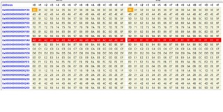
2. After the burning failed, read the burning content and found that there is a phenomenon, that is, the value of 16 BYTE is 0xFF every time, that is, the writing is not successful. It seems that the problem is Fapi_BlockProgram, in red font The two judgment conditions were added by me. They are improved but errors still occur.

uint32_t Fapi_BlockProgram( uint32_t Bank, uint32_t Flash_Address, uint32_t Data_Address, uint32_t SizeInBytes)
{
register uint32_t src = Data_Address;
register uint32_t dst = Flash_Address;
uint32_t bytes;

if (SizeInBytes < 16)
bytes = SizeInBytes;
else
bytes = 16;

if ((Fapi_initializeFlashBanks((uint32_t)SYS_CLK_FREQ)) == Fapi_Status_Success)

{
(void)Fapi_setActiveFlashBank((Fapi_FlashBankType)Bank);
(void)Fapi_enableMainBankSectors(0x0FFF); /* used for API 2.01*/
}

else {
return (1);
}

while( FAPI_CHECK_FSM_READY_BUSY != Fapi_Status_FsmReady );
while( FAPI_GET_FSM_STATUS != Fapi_Status_Success );

while( SizeInBytes > 0)
{
             Fapi_issueProgrammingCommand((uint32_t *)dst,
                                                                      (uint8_t *)src,
                                                                      (uint32_t) bytes,
                                                                       0,
                                                                       0,
                                                                       Fapi_AutoEccGeneration);

while( FAPI_CHECK_FSM_READY_BUSY == Fapi_Status_FsmBusy );
while(FAPI_GET_FSM_STATUS != Fapi_Status_Success);
while( FAPI_CHECK_FSM_READY_BUSY != Fapi_Status_FsmReady );


src += bytes;
dst += bytes;
SizeInBytes -= bytes;
if (SizeInBytes < 16)

   {
      bytes = SizeInBytes;
    }
 }

//status =  Flash_Program_Check(Flash_Address, Data_Address, SizeInBytes);
return (0);
}

The questions I want to ask are the following:

1. How to confirm that the programming has been successful after burning 16 BYTEs each time?

2. If I execute Flash_Program_Check() every time after burning 16 BYTEs, what status do I need to set or check first, or do I need to delay it for a period of time?

3. Currently, every time I receive 2048 Byte data, I start burning. Is there a limit to the size of this temporary storage area? I ask this because I will continue to write after receiving 2048 Byte data until burning. After completion, receive the next 2048 Byte

4. What MHZ should be set to SYS_CLK_FREQ? It is currently set at 64MHZ.

5. Why does adjusting SYS_CLK_FREQ affect the success rate of programming (adjustment range 32MHz ~ 80MHz)

6. Why does Flash_Program_Check fail to execute after judging that Fapi_Status_Success has been successful?

Please, is there anyone who can help me? I would be very grateful.

PS:When reading the FLASH content when an error occurs, 16 consecutive BYTEs will be sent, but none of them are written.

  • 1. How to confirm that the programming has been successful after burning 16 BYTEs each time?

    If the error flag is not set (FSM status), the data should be programmed successfully. You don't have to read the data back, then compare.

    2. If I execute Flash_Program_Check() every time after burning 16 BYTEs, what status do I need to set or check first, or do I need to delay it for a period of time?

    No delay is needed because yo are checking the FSM status and FSM Busy flag.

    3. Currently, every time I receive 2048 Byte data, I start burning. Is there a limit to the size of this temporary storage area? I ask this because I will continue to write after receiving 2048 Byte data until burning. After completion, receive the next 2048 Byte

    No limitation. The flash bank bus width is 128 bits + 16 bit ECC, so the API only takes 16 bytes every time. The supplied starting address to program at plus the data buffer length (maximum 16 bytes) cannot exceed the bank data width (128 bits).

    4. What MHZ should be set to SYS_CLK_FREQ? It is currently set at 64MHZ.

    It is system clock: 100Mhz. Do you program the flash wait states properly. It is 1 for 100Mhz , please refer to datasheet.

    5. Why does adjusting SYS_CLK_FREQ affect the success rate of programming (adjustment range 32MHz ~ 80MHz)

    I don't recommend adjusting the frequency dynamically. Please use the system clock for flash operation. The flash can support zero address and data wait states up to a CPU speed of 50 MHz in nonpipelined mode. The flash supports a maximum CPU clock speed of 100 MHz in pipelined mode for the PZ package.

    6. Why does Flash_Program_Check fail to execute after judging that Fapi_Status_Success has been successful?

    I am not sure what happens. How many units have this problem? Has the flash been erased before programming?

  • Hello:
    Things have improved a bit. Thank you for your help. I would like to ask again:
    1. What is the error flag after each 16 BYTE burning?
    Fapi_StatusType
    typedef enum
    {
    Fapi_Status_Success=0, /* Function completed successfully */
    Fapi_Status_FsmBusy, /* FSM is Busy */
    Fapi_Status_FsmReady, /* FSM is Ready */
    Fapi_Error_Fail, /* Generic Function Fail code */
    Fapi_Error_NullPointer, /* One of the pointer parameters is a null pointer */
    Fapi_Error_InvalidCommand, /* Command used is invalid for the function called */
    Fapi_Error_InvalidEccAddress, /* Returned if the ECC Address given to a function is invalid for that function */
    Fapi_Error_OtpChecksumMismatch, /* Returned if OTP checksum does not match expected value */
    Fapi_Error_InvalidHclkValue, /* Returned if FClk is above max FClk value -FClk is a calculated from HClk and RWAIT/EWAIT */
    Fapi_Error_InvalidBank, /* Returned if the specified bank does not exist */
    Fapi_Error_InvalidAddress, /* Returned if the specified Address does not exist in Flash or OTP */
    Fapi_Error_InvalidReadMode, /* Returned if the specified read mode does not exist */
    Fapi_Error_AsyncIncorrectDataBufferLength, /* Returned if Data buffer size specified exceeds Data bank width */
    Fapi_Error_AsyncIncorrectEccBufferLength, /* Returned if ECC buffer size specified exceeds ECC bank width */
    Fapi_Error_AsyncDataEccBufferLengthMismatch, /* Returned if Data buffer size either is not 64bit aligned or Data length exceeds amount ECC supplied */
    Fapi_Error_FeatureNotAvailable /* FMC feature is not available on this device */
    } ATTRIBUTE_PACKED Fapi_StatusType;

    2. Before burning the program, confirm that the flash memory has been erased and checked to see if it is 0xFFFFFFFF. Failure to burn successfully means that the status flag has timed out (more than 20 seconds) or there are 16 consecutive BYTEs that have not been written. , or maintain 0xFF, is there any solution?

    Thank you again for your assistance.

  • Hi Weeken,

    How many devices failed?

    Can you please check if CCS or uniflash can program a file to this location (16 bytes) properly?

  • Hello:
    What is more incomprehensible about the current situation is that if it cannot be programmed or a programming error occurs, I only need to change the SYS_CLK_FREQ frequency setting in the bl_config.h file (at 32MHz~64MHz) and the other programs will not change. After assembling the program, you can successfully execute the BOOTLOADER function and burn the program into the MCU.

  • Hi Weeken,

    Can you please share the two halcogen files with me for checking your clock configurations?

  • I did not use halcogen to set any functions, I only used the SPN192 sample program to make modifications.

  • Hi Weeken,

    I understood. How about system.c? I'd like to check the PLL settings.

  • //*****************************************************************************
    //
    // system.c    : Functions to configure PLL, and peripherals
    // Author      : QJ Wang. qjwang@ti.com
    // Date        : 9-19-2012
    //
    // Copyright (c) 2008-2011 Texas Instruments Incorporated.  All rights reserved.
    // Software License Agreement
    //
    // Texas Instruments (TI) is supplying this software for use solely and
    // exclusively on TI's microcontroller products. The software is owned by
    // TI and/or its suppliers, and is protected under applicable copyright
    // laws. You may not combine this software with "viral" open-source
    // software in order to form a larger program.
    //
    // THIS SOFTWARE IS PROVIDED "AS IS" AND WITH ALL FAULTS.
    // NO WARRANTIES, WHETHER EXPRESS, IMPLIED OR STATUTORY, INCLUDING, BUT
    // NOT LIMITED TO, IMPLIED WARRANTIES OF MERCHANTABILITY AND FITNESS FOR
    // A PARTICULAR PURPOSE APPLY TO THIS SOFTWARE. TI SHALL NOT, UNDER ANY
    // CIRCUMSTANCES, BE LIABLE FOR SPECIAL, INCIDENTAL, OR CONSEQUENTIAL
    // DAMAGES, FOR ANY REASON WHATSOEVER.
    //
    //*****************************************************************************
    /* Include Files */
    
    #include "system.h"
    #include "bl_config.h"
    
    //#include "sys_selftest.h"
    //#include "pinmux.h"
    
    /* USER CODE BEGIN (1) */
    /* USER CODE END */
    
    /** @fn void systemInit(void)
    *   @brief Initializes System Driver
    *
    *   This function initializes the System driver.
    *
    */
    
    /* USER CODE BEGIN (2) */
    /* USER CODE END */
    
    void setupPLL(void)
    {
    
    /* USER CODE BEGIN (3) */
    /* USER CODE END */
    
        /** - Configure PLL control registers */
        /** @b Initialize @b Pll1: */
    
        /**   - Setup pll control register 1:
        *     - Setup reset on oscillator slip
        *     - Setup bypass on pll slip
        *     - setup Pll output clock divider to max before Lock
        *     - Setup reset on oscillator fail
        *     - Setup reference clock divider
        *     - Setup Pll multiplier
        */
        systemREG1->PLLCTL1 =  0x00000000U
                            |  0x20000000U
                            | ((0x1F)<< 24U)
                            |  0x00000000U
                            | ((6U - 1U)<< 16U)
                            | ((120U - 1U)<< 8U);
    
        /**   - Setup pll control register 2
        *     - Enable/Disable frequency modulation
        *     - Setup spreading rate
        *     - Setup bandwidth adjustment
        *     - Setup internal Pll output divider
        *     - Setup spreading amount
        */
        systemREG1->PLLCTL2 =  0x00000000U
                            | (255U << 22U)
                            | (7U << 12U)
                            | ((2U - 1U)<< 9U)
                            |  61U;
    
        /** @b Initialize @b Pll2: */
    
        /**   - Setup pll2 control register :
        *     - setup Pll output clock divider to max before Lock
        *     - Setup reference clock divider
        *     - Setup internal Pll output divider
        *     - Setup Pll multiplier
        */
        systemREG2->PLLCTL3 = ((2U - 1U) << 29U)
                            | ((0x1F)<< 24U)
                            | ((5U - 1U)<< 16U)
                            | ((30U - 1U) << 8U);
    
        /** - Enable PLL(s) to start up or Lock */
        systemREG1->CSDIS = 0x00000000U
                          | 0x00000000U
                          | 0x00000008U
                          | 0x00000080U
                          | 0x00000000U
                          | 0x00000000U
                          | 0x00000000U;
    }
    
    void trimLPO(void)
    {
    
    /* USER CODE BEGIN (4) */
    /* USER CODE END */
    
        /** @b Initialize Lpo: */
        /** Load TRIM values from OTP if present else load user defined values */
        if(LPO_TRIM_VALUE != 0xFFFF)
        {
    
            systemREG1->LPOMONCTL  = (1U << 24U)
                                    | LPO_TRIM_VALUE;
        }
        else
        {
    
            systemREG1->LPOMONCTL   = (1U << 24U)
                                     | (16U << 8U)
                                     | 8U;
        }
    
    /* USER CODE BEGIN (5) */
    /* USER CODE END */
    
    }
    
    void setupFlash(void)
    {
    
    /* USER CODE BEGIN (6) */
    /* USER CODE END */
    
        /** - Setup flash read mode, address wait states and data wait states */
        flashWREG->FRDCNTL =  0x00000000U
    #if defined(TMS570LS04) || defined(RM42)
                           | (1U << 8U)
                           | (0U << 4U)
    #else
                           | (3U << 8U)
                           | (1U << 4U)
    #endif
                           |  1U;
    
        /** - Setup flash access wait states for bank 7 */
        FSM_WR_ENA = 0x5;
        EEPROM_CONFIG = 0x00030002;
    
    /* USER CODE BEGIN (7) */
    /* USER CODE END */
    
        /** - Disable write access to flash state machine registers */
        FSM_WR_ENA = 0xA;
    
        /** - Setup flash bank power modes */
        flashWREG->FBFALLBACK = 0x00000000
                              | (SYS_ACTIVE << 14U)
                              | (SYS_SLEEP << 12U)
                              | (SYS_SLEEP << 10U)
                              | (SYS_SLEEP << 8U)
                              | (SYS_SLEEP << 6U)
                              | (SYS_SLEEP << 4U)
    #if defined(TMS570LS04) || defined(RM42)
                              | (SYS_SLEEP << 2U)
    #else
                              | (SYS_ACTIVE << 2U)
    #endif
                              |  SYS_ACTIVE;
    
    /* USER CODE BEGIN (8) */
    /* USER CODE END */
    
    }
    
    void periphInit(void)
    {
    
    /* USER CODE BEGIN (9) */
    /* USER CODE END */
    
        /** - Disable Peripherals before peripheral powerup*/
        systemREG1->PENA = 0U;
    
        /** - Release peripherals from reset and enable clocks to all peripherals */
        /** - Power-up all peripharals */
        pcrREG->PSPWRDWNCLR0 = 0xFFFFFFFFU;
        pcrREG->PSPWRDWNCLR1 = 0xFFFFFFFFU;
        pcrREG->PSPWRDWNCLR2 = 0xFFFFFFFFU;
        pcrREG->PSPWRDWNCLR3 = 0xFFFFFFFFU;
    
        /** - Enable Peripherals */
        systemREG1->PENA = 1U;
    
    /* USER CODE BEGIN (10) */
    /* USER CODE END */
    
    }
    
    void mapClocks(void)
    {
    
    /* USER CODE BEGIN (11) */
    /* USER CODE END */
    
        /** @b Initialize @b Clock @b Tree: */
        /** - Diable / Enable clock domain */
        systemREG1->CDDIS= (FALSE << 4 ) /* AVCLK 1 OFF */
                          |(TRUE << 5 ) /* AVCLK 2 OFF */
                          |(FALSE << 8 ) /* VCLK3 OFF */
                          |(FALSE << 10) /* AVCLK 3 OFF */
                          |(FALSE << 11); /* AVCLK 4 OFF */
    
        /** - Wait for until clocks are locked */
        while ((systemREG1->CSVSTAT & ((systemREG1->CSDIS ^ 0xFF) & 0xFF)) != ((systemREG1->CSDIS ^ 0xFF) & 0xFF))
        {
        }
    //    while (!(systemREG1->CSVSTAT & 0x040));
    
    /* USER CODE BEGIN (12) */
    /* USER CODE END */
    
        /* Now the PLLs are locked and the PLL outputs can be sped up */
        /* The R-divider was programmed to be 0xF. Now this divider is changed to programmed value */
    #if defined(TMS570LS04) || defined(RM42)
        systemREG1->PLLCTL1 = (systemREG1->PLLCTL1 & 0xE0FFFFFF)|((2U - 1U)<< 24U);
    #else
        systemREG1->PLLCTL1 = (systemREG1->PLLCTL1 & 0xE0FFFFFF)|((1U - 1U)<< 24U);
    #endif
        systemREG2->PLLCTL3 = (systemREG2->PLLCTL3 & 0xE0FFFFFF)|((1U - 1U)<< 24U);
    
        /** - Map device clock domains to desired sources and configure top-level dividers */
        /** - All clock domains are working off the default clock sources until now */
        /** - The below assignments can be easily modified using the HALCoGen GUI */
    
        /** - Setup GCLK, HCLK and VCLK clock source for normal operation, power down mode and after wakeup */
        systemREG1->GHVSRC = (SYS_PLL1 << 24U)
                           | (SYS_PLL1 << 16U)
                           |  SYS_PLL1;
    
        /** - Setup synchronous peripheral clock dividers for VCLK1, VCLK2, VCLK3 */
    #if defined(TMS570LS04) || defined(RM42)
        systemREG1->VCLKR   = 1;   //1U;
        systemREG1->VCLK2R  = 1;    //1U;
        systemREG2->VCLK3R  = 1U;
    #else
        systemREG1->VCLKR   = 1;   //1U;
        systemREG1->VCLK2R  = 1;    //1U;
        systemREG2->VCLK3R  = 1U;
    #endif
    /* USER CODE BEGIN (13) */
    /* USER CODE END */
    
        /** - Setup RTICLK1 and RTICLK2 clocks */
        systemREG1->RCLKSRC = (1U << 24U)
                            | (SYS_VCLK << 16U)
                            | (1U << 8U)
                            |  SYS_VCLK;
    
        /** - Setup asynchronous peripheral clock sources for AVCLK1 and AVCLK2 */
        systemREG1->VCLKASRC = (SYS_VCLK << 8U)
                              |  SYS_VCLK;
    
        systemREG2->VCLKACON1 = (1U << 24)
                               | 1 << 20U
                               | (SYS_VCLK << 16)
                               | (1U << 8)
                               | 1 << 4U
    #if defined(TMS570LS04) || defined(RM42)
                               | SYS_VCLK;
    #else
                               | SYS_PLL2;
    #endif
    /* USER CODE BEGIN (14) */
    /* USER CODE END */
    
    }
    
    void systemInit(void)
    {
    /* USER CODE BEGIN (15) */
    /* USER CODE END */
    
        /* Configure PLL control registers and enable PLLs.
         * The PLL takes (127 + 1024 * NR) oscillator cycles to acquire lock.
         * This initialization sequence performs all the tasks that are not
         * required to be done at full application speed while the PLL locks.
         */
        setupPLL();
    
    
    /* USER CODE BEGIN (17) */
    /* USER CODE END */
    
        /* Enable clocks to peripherals and release peripheral reset */
        periphInit();
    
    /* USER CODE BEGIN (18) */
    /* USER CODE END */
    
    
    /* USER CODE BEGIN (20) */
    /* USER CODE END */
    
        /** - Set up flash address and data wait states based on the target CPU clock frequency
         * The number of address and data wait states for the target CPU clock frequency are specified
         * in the specific part's datasheet.
         */
        setupFlash();
    
    /* USER CODE BEGIN (21) */
    /* USER CODE END */
    
        /** - Configure the LPO such that HF LPO is as close to 10MHz as possible */
        trimLPO();
    
    /* USER CODE BEGIN (23) */
    /* USER CODE END */
    
        /** - Wait for PLLs to start up and map clock domains to desired clock sources */
        //mapClocks();
    
    /* USER CODE BEGIN (24) */
    /* USER CODE END */
    
        /** - set ECLK pins functional mode */
        systemREG1->SYSPC1 = 0U;
    
        /** - set ECLK pins default output value */
        systemREG1->SYSPC4 = 0U;
    
        /** - set ECLK pins output direction */
        systemREG1->SYSPC2 = 1U;
    
        /** - set ECLK pins open drain enable */
        systemREG1->SYSPC7 = 0U;
    
        /** - set ECLK pins pullup/pulldown enable */
        systemREG1->SYSPC8 = 0U;
    
        /** - set ECLK pins pullup/pulldown select */
        systemREG1->SYSPC9 = 1U;
    
        /** - Setup ECLK */
        systemREG1->ECPCNTL = (0U << 24U)
                            | (0U << 23U)
                            | ((8U - 1U) & 0xFFFFU);
    
    /* USER CODE BEGIN (25) */
    /* USER CODE END */
    }
    
    void systemPowerDown(uint32_t mode)
    {
    
    /* USER CODE BEGIN (26) */
    /* USER CODE END */
    
        /* Disable clock sources */
        systemREG1->CSDISSET = mode & 0x000000FFU;
    
        /* Disable clock domains */
        systemREG1->CDDIS = (mode >> 8U) & 0x00000FFFU;
    
        /* Idle CPU */
        asm(" wfi");
    
    /* USER CODE BEGIN (27) */
    /* USER CODE END */
    
    }
    
    /* USER CODE BEGIN (28) */
    /* USER CODE END */
    

    This is the system.c currently used. Please help to check if there are any setting errors. Thank you.

  • Hi Weeken,

    The PLL settings are not proper for TMS570LS0714 PZ package. I think this file was designed for PGE package which supports CPU speed up to 160MHz. The maximum CPU speed of LS0714 PZ package is 100MHz.

    Please try this system.c

    /** @file system.c
    *   @brief System Driver Source File
    *   @date 11-Dec-2018
    *   @version 04.07.01
    *
    *   This file contains:
    *   - API Functions
    *   .
    *   which are relevant for the System driver.
    */
    
    /*
    * Copyright (C) 2009-2018 Texas Instruments Incorporated - www.ti.com
    *
    *
    *  Redistribution and use in source and binary forms, with or without
    *  modification, are permitted provided that the following conditions
    *  are met:
    *
    *    Redistributions of source code must retain the above copyright
    *    notice, this list of conditions and the following disclaimer.
    *
    *    Redistributions in binary form must reproduce the above copyright
    *    notice, this list of conditions and the following disclaimer in the
    *    documentation and/or other materials provided with the
    *    distribution.
    *
    *    Neither the name of Texas Instruments Incorporated nor the names of
    *    its contributors may be used to endorse or promote products derived
    *    from this software without specific prior written permission.
    *
    *  THIS SOFTWARE IS PROVIDED BY THE COPYRIGHT HOLDERS AND CONTRIBUTORS
    *  "AS IS" AND ANY EXPRESS OR IMPLIED WARRANTIES, INCLUDING, BUT NOT
    *  LIMITED TO, THE IMPLIED WARRANTIES OF MERCHANTABILITY AND FITNESS FOR
    *  A PARTICULAR PURPOSE ARE DISCLAIMED. IN NO EVENT SHALL THE COPYRIGHT
    *  OWNER OR CONTRIBUTORS BE LIABLE FOR ANY DIRECT, INDIRECT, INCIDENTAL,
    *  SPECIAL, EXEMPLARY, OR CONSEQUENTIAL DAMAGES (INCLUDING, BUT NOT
    *  LIMITED TO, PROCUREMENT OF SUBSTITUTE GOODS OR SERVICES; LOSS OF USE,
    *  DATA, OR PROFITS; OR BUSINESS INTERRUPTION) HOWEVER CAUSED AND ON ANY
    *  THEORY OF LIABILITY, WHETHER IN CONTRACT, STRICT LIABILITY, OR TORT
    *  (INCLUDING NEGLIGENCE OR OTHERWISE) ARISING IN ANY WAY OUT OF THE USE
    *  OF THIS SOFTWARE, EVEN IF ADVISED OF THE POSSIBILITY OF SUCH DAMAGE.
    *
    */
    
    
    /* USER CODE BEGIN (0) */
    /* USER CODE END */
    
    
    /* Include Files */
    
    #include "system.h"
    #include "sys_selftest.h"
    #include "sys_pcr.h"
    #include "pinmux.h"
    
    /* USER CODE BEGIN (1) */
    /* USER CODE END */
    
    /** @fn void systemInit(void)
    *   @brief Initializes System Driver
    *
    *   This function initializes the System driver.
    *
    */
    
    /* USER CODE BEGIN (2) */
    /* USER CODE END */
    
    /* SourceId : SYSTEM_SourceId_001 */
    /* DesignId : SYSTEM_DesignId_001 */
    /* Requirements : HL_SR451 */
    void setupPLL(void)
    {
    
    /* USER CODE BEGIN (3) */
    /* USER CODE END */
    
        /* Disable PLL1 */
        systemREG1->CSDISSET = 0x00000002U;
        /*SAFETYMCUSW 28 D MR:NA <APPROVED> "Hardware status bit read check" */
        while((systemREG1->CSDIS & 0x2U) != 0x2U)
        {
        /* Wait */
        }
    
        /* Clear Global Status Register */
        systemREG1->GBLSTAT = 0x301U;
    
        /** - Configure PLL control registers */
        /** @b Initialize @b Pll1: */
    
        /**   - Setup pll control register 1:
        *     - Setup reset on oscillator slip
        *     - Setup bypass on pll slip
        *     - setup Pll output clock divider to max before Lock
        *     - Setup reset on oscillator fail
        *     - Setup reference clock divider
        *     - Setup Pll multiplier
        */
        systemREG1->PLLCTL1 =  (uint32)0x00000000U
                            |  (uint32)0x20000000U
                            |  (uint32)((uint32)0x1FU << 24U)
                            |  (uint32)0x00000000U
                            |  (uint32)((uint32)(6U - 1U)<< 16U)
                            |  (uint32)(0x9500U);
    
        /**   - Setup pll control register 2
        *     - Setup spreading rate
        *     - Setup bandwidth adjustment
        *     - Setup internal Pll output divider
        *     - Setup spreading amount
        */
        systemREG1->PLLCTL2 =  (uint32)((uint32)255U << 22U)
                            |  (uint32)((uint32)7U << 12U)
                            |  (uint32)((uint32)(2U - 1U) << 9U)
                            |  (uint32)61U;
    
        /** - Enable PLL(s) to start up or Lock */
        systemREG1->CSDIS = 0x00000000U
                          | 0x00000000U
                          | 0x00000008U
                          | 0x00000080U
                          | 0x00000000U
                          | 0x00000040U
                          | 0x00000000U;
    }
    
    /** @fn void trimLPO(void)
    *   @brief Initialize LPO trim values
    *
    *   Load TRIM values from OTP if present else call customTrimLPO() function
    *
    */
    /* SourceId : SYSTEM_SourceId_002 */
    /* DesignId : SYSTEM_DesignId_002 */
    /* Requirements : HL_SR468 */
    void trimLPO(void)
    {
        uint32 u32clocktestConfig;
        /* Save user clocktest register configuration */
        u32clocktestConfig = systemREG1->CLKTEST;
    /* USER CODE BEGIN (4) */
    /* USER CODE END */
        /*The TRM states OTP TRIM value should be stepped to avoid large changes in the HF LPO clock that would result in a LPOCLKMON fault. At issue is the TRM does not specify what the maximum step is so there is no metric to use for the SW implementation - the routine can temporarily disable the LPOCLKMON range check so the sudden change will not cause a fault.*/
        /* Disable clock range detection*/
        systemREG1->CLKTEST = (systemREG1->CLKTEST 
                            | (uint32)((uint32)0x1U << 24U))        
                            & (uint32)(~((uint32)0x1U << 25U));                       
     
        /*SAFETYMCUSW 139 S MR:13.7 <APPROVED> "Hardware status bit read check" */
        if(LPO_TRIM_VALUE != 0xFFFFU)
        {
    
            systemREG1->LPOMONCTL  = (uint32)((uint32)1U << 24U)
                                   | (uint32)((uint32)LPO_TRIM_VALUE);
        }
        else
        {
        
            customTrimLPO();
            
        }
        
        /* Restore the user clocktest register value configuration */
        systemREG1->CLKTEST = u32clocktestConfig;
    
    /* USER CODE BEGIN (5) */
    /* USER CODE END */
    
    }
    
    /* SourceId : SYSTEM_SourceId_003 */
    /* DesignId : SYSTEM_DesignId_003 */
    /* Requirements : HL_SR457 */
    void setupFlash(void)
    {
    
    /* USER CODE BEGIN (6) */
    /* USER CODE END */
    
        /** - Setup flash read mode, address wait states and data wait states */
        flashWREG->FRDCNTL =  0x00000000U
                           | (uint32)((uint32)1U << 8U)
                           | (uint32)((uint32)0U << 4U)
                           |  1U;
    
        /** - Setup flash access wait states for bank 7 */
        FSM_WR_ENA_HL    = 0x5U;
        EEPROM_CONFIG_HL = 0x00000002U
                         | (uint32)((uint32)5U << 16U) ;
    
    /* USER CODE BEGIN (7) */
    /* USER CODE END */
    
        /** - Disable write access to flash state machine registers */
        FSM_WR_ENA_HL    = 0xAU;
    
        /** - Setup flash bank power modes */
        flashWREG->FBFALLBACK = 0x00000000U
                              | (uint32)((uint32)SYS_ACTIVE << 14U) /* BANK 7 */
                              | (uint32)((uint32)SYS_ACTIVE << 0U); /* BANK 0 */
    
    /* USER CODE BEGIN (8) */
    /* USER CODE END */
    
    }
    
    /* SourceId : SYSTEM_SourceId_004 */
    /* DesignId : SYSTEM_DesignId_004 */
    /* Requirements : HL_SR470 */
    void periphInit(void)
    {
    
    /* USER CODE BEGIN (9) */
    /* USER CODE END */
    
        /** - Disable Peripherals before peripheral powerup*/
        systemREG1->CLKCNTL &= 0xFFFFFEFFU;
    
        /** - Release peripherals from reset and enable clocks to all peripherals */
        /** - Power-up all peripherals */
        pcrREG->PSPWRDWNCLR0 = 0xFFFFFFFFU;
        pcrREG->PSPWRDWNCLR1 = 0xFFFFFFFFU;
        pcrREG->PSPWRDWNCLR2 = 0xFFFFFFFFU;
        pcrREG->PSPWRDWNCLR3 = 0xFFFFFFFFU;
    
        /** - Enable Peripherals */
        systemREG1->CLKCNTL |= 0x00000100U;
    
    /* USER CODE BEGIN (10) */
    /* USER CODE END */
    
    }
    
    /* SourceId : SYSTEM_SourceId_005 */
    /* DesignId : SYSTEM_DesignId_005 */
    /* Requirements : HL_SR469 */
    void mapClocks(void)
    {
        uint32 SYS_CSVSTAT, SYS_CSDIS;
    
    /* USER CODE BEGIN (11) */
    /* USER CODE END */
    
        /** @b Initialize @b Clock @b Tree: */
        /** - Disable / Enable clock domain */
        systemREG1->CDDIS = (uint32)((uint32)0U << 4U ) /* AVCLK1 , 1 - OFF, 0 - ON */
                          | (uint32)((uint32)0U << 5U ) /* AVCLK2 , 1 - OFF, 0 - ON */
                          | (uint32)((uint32)0U << 8U ) /* VCLK3 , 1 - OFF, 0 - ON */
                          | (uint32)((uint32)0U << 9U ) /* VCLK4 , 1 - OFF, 0 - ON */
                          | (uint32)((uint32)1U << 10U) /* AVCLK3 , 1 - OFF, 0 - ON */
                          | (uint32)((uint32)0U << 11U); /* AVCLK4 , 1 - OFF, 0 - ON */
    
    
        /* Work Around for Errata SYS#46:
         *
         * Errata Description:
         *            Clock Source Switching Not Qualified with Clock Source Enable And Clock Source Valid
         * Workaround:
         *            Always check the CSDIS register to make sure the clock source is turned on and check
         * the CSVSTAT register to make sure the clock source is valid. Then write to GHVSRC to switch the clock.
         */
        /** - Wait for until clocks are locked */
        SYS_CSVSTAT = systemREG1->CSVSTAT;
        SYS_CSDIS = systemREG1->CSDIS;
        while ((SYS_CSVSTAT & ((SYS_CSDIS ^ 0xFFU) & 0xFFU)) != ((SYS_CSDIS ^ 0xFFU) & 0xFFU))
        {
            SYS_CSVSTAT = systemREG1->CSVSTAT;
            SYS_CSDIS = systemREG1->CSDIS;
        } /* Wait */
    
    /* USER CODE BEGIN (12) */
    /* USER CODE END */
    
        /** - Map device clock domains to desired sources and configure top-level dividers */
        /** - All clock domains are working off the default clock sources until now */
        /** - The below assignments can be easily modified using the HALCoGen GUI */
    
        /** - Setup GCLK, HCLK and VCLK clock source for normal operation, power down mode and after wakeup */
        systemREG1->GHVSRC = (uint32)((uint32)SYS_OSC << 24U)
                           | (uint32)((uint32)SYS_OSC << 16U)
                           | (uint32)((uint32)SYS_PLL1 << 0U);
    
        /** - Setup RTICLK1 and RTICLK2 clocks */
        systemREG1->RCLKSRC = (uint32)((uint32)1U << 24U)
                            | (uint32)((uint32)SYS_VCLK << 16U)
                            | (uint32)((uint32)1U << 8U)
                            | (uint32)((uint32)SYS_VCLK << 0U);
    
        /** - Setup asynchronous peripheral clock sources for AVCLK1 and AVCLK2 */
        systemREG1->VCLKASRC = (uint32)((uint32)SYS_VCLK << 8U)
                             | (uint32)((uint32)SYS_VCLK << 0U);
    
        /** - Setup synchronous peripheral clock dividers for VCLK1, VCLK2, VCLK3 */
        systemREG1->CLKCNTL  = (systemREG1->CLKCNTL & 0xF0FFFFFFU)
                             | (uint32)((uint32)0U << 24U);
        systemREG1->CLKCNTL  = (systemREG1->CLKCNTL & 0xFFF0FFFFU)
                             | (uint32)((uint32)0U << 16U);
    
        systemREG2->CLK2CNTL = (systemREG2->CLK2CNTL & 0xFFFFF0FFU)
                             | (uint32)((uint32)0U << 8U);
    
    /* USER CODE BEGIN (13) */
    /* USER CODE END */
    
        /* Now the PLLs are locked and the PLL outputs can be sped up */
        /* The R-divider was programmed to be 0xF. Now this divider is changed to programmed value */
        systemREG1->PLLCTL1 = (systemREG1->PLLCTL1 & 0xE0FFFFFFU) | (uint32)((uint32)(2U - 1U) << 24U);
    
        /* Enable/Disable Frequency modulation */
        systemREG1->PLLCTL2 |= 0x00000000U;
    
    /* USER CODE BEGIN (14) */
    /* USER CODE END */
    
    }
    
    /* SourceId : SYSTEM_SourceId_006 */
    /* DesignId : SYSTEM_DesignId_006 */
    /* Requirements : HL_SR471 */
    void systemInit(void)
    {
        uint32 efcCheckStatus;
    
    /* USER CODE BEGIN (15) */
    /* USER CODE END */
    
        /* Configure PLL control registers and enable PLLs.
         * The PLL takes (127 + 1024 * NR) oscillator cycles to acquire lock.
         * This initialization sequence performs all the tasks that are not
         * required to be done at full application speed while the PLL locks.
         */
        setupPLL();
    
    /* USER CODE BEGIN (16) */
    /* USER CODE END */
    
        /* Run eFuse controller start-up checks and start eFuse controller ECC self-test.
         * This includes a check for the eFuse controller error outputs to be stuck-at-zero.
         */
        efcCheckStatus = efcCheck();
    
    /* USER CODE BEGIN (17) */
    /* USER CODE END */
    
        /* Enable clocks to peripherals and release peripheral reset */
        periphInit();
    
    /* USER CODE BEGIN (18) */
    /* USER CODE END */
    
        /* Configure device-level multiplexing and I/O multiplexing */
        muxInit();
    
    /* USER CODE BEGIN (19) */
    /* USER CODE END */
    
        if(efcCheckStatus == 0U)
        {
            /* Wait for eFuse controller self-test to complete and check results */
            if (checkefcSelfTest() == FALSE)                            /* eFuse controller ECC logic self-test failed */
            {
                selftestFailNotification(EFCCHECK_FAIL1);           /* device operation is not reliable */
            }
        }
        else if(efcCheckStatus == 2U)
        {
            /* Wait for eFuse controller self-test to complete and check results */
            if (checkefcSelfTest() == FALSE)                            /* eFuse controller ECC logic self-test failed */
            {
                selftestFailNotification(EFCCHECK_FAIL1);           /* device operation is not reliable */
            }
            else
            {
                selftestFailNotification(EFCCHECK_FAIL2);
            }
        }
        else
        {
        /* Empty */
        }
    /* USER CODE BEGIN (20) */
    /* USER CODE END */
    
        /** - Set up flash address and data wait states based on the target CPU clock frequency
         * The number of address and data wait states for the target CPU clock frequency are specified
         * in the specific part's datasheet.
         */
        setupFlash();
    
    /* USER CODE BEGIN (21) */
    /* USER CODE END */
    
        /** - Configure the LPO such that HF LPO is as close to 10MHz as possible */
        trimLPO();
    
    
    /* USER CODE BEGIN (23) */
    /* USER CODE END */
    
        /** - Wait for PLLs to start up and map clock domains to desired clock sources */
        mapClocks();
    
    /* USER CODE BEGIN (24) */
    /* USER CODE END */
    
        /** - set ECLK pins functional mode */
        systemREG1->SYSPC1 = 0U;
    
        /** - set ECLK pins default output value */
        systemREG1->SYSPC4 = 0U;
    
        /** - set ECLK pins output direction */
        systemREG1->SYSPC2 = 1U;
    
        /** - set ECLK pins open drain enable */
        systemREG1->SYSPC7 = 0U;
    
        /** - set ECLK pins pullup/pulldown enable */
        systemREG1->SYSPC8 = 0U;
    
        /** - set ECLK pins pullup/pulldown select */
        systemREG1->SYSPC9 = 1U;
    
        /** - Setup ECLK */
        systemREG1->ECPCNTL = (uint32)((uint32)0U << 24U)
                            | (uint32)((uint32)0U << 23U)
                            | (uint32)((uint32)(8U - 1U) & 0xFFFFU);
    
    /* USER CODE BEGIN (25) */
    /* USER CODE END */
    }
    
    /* SourceId : SYSTEM_SourceId_007 */
    /* DesignId : SYSTEM_DesignId_007 */
    /* Requirements : HL_SR493 */
    void systemPowerDown(uint32 mode)
    {
    
    /* USER CODE BEGIN (26) */
    /* USER CODE END */
    
        /* Disable clock sources */
        systemREG1->CSDISSET = mode & 0x000000FFU;
    
        /* Disable clock domains */
        systemREG1->CDDIS = (mode >> 8U) & 0x00000FFFU;
    
        /* Idle CPU */
        _gotoCPUIdle_();
    
    /* USER CODE BEGIN (27) */
    /* USER CODE END */
    
    }
    
    /* USER CODE BEGIN (28) */
    /* USER CODE END */
    
    /** @fn void systemGetConfigValue(system_config_reg_t *config_reg, config_value_type_t type)
    *   @brief Get the initial or current values of the configuration registers
    *
    *   @param[in] *config_reg: pointer to the struct to which the initial or current value of the configuration registers need to be stored
    *   @param[in] type:    whether initial or current value of the configuration registers need to be stored
    *                       - InitialValue: initial value of the configuration registers will be stored in the struct pointed by config_reg
    *                       - CurrentValue: initial value of the configuration registers will be stored in the struct pointed by config_reg
    *
    *   This function will copy the initial or current value (depending on the parameter 'type') of the configuration registers to the struct pointed by config_reg
    *
    */
    /* SourceId : SYSTEM_SourceId_008 */
    /* DesignId : SYSTEM_DesignId_008 */
    /* Requirements : HL_SR506 */
    void systemGetConfigValue(system_config_reg_t *config_reg, config_value_type_t type)
    {
        if (type == InitialValue)
        {
            config_reg->CONFIG_SYSPC1 = SYS_SYSPC1_CONFIGVALUE;
            config_reg->CONFIG_SYSPC2 = SYS_SYSPC2_CONFIGVALUE;
            config_reg->CONFIG_SYSPC7 = SYS_SYSPC7_CONFIGVALUE;
            config_reg->CONFIG_SYSPC8 = SYS_SYSPC8_CONFIGVALUE;
            config_reg->CONFIG_SYSPC9 = SYS_SYSPC9_CONFIGVALUE;
            config_reg->CONFIG_CSDIS = SYS_CSDIS_CONFIGVALUE;
            config_reg->CONFIG_CDDIS = SYS_CDDIS_CONFIGVALUE;
            config_reg->CONFIG_GHVSRC = SYS_GHVSRC_CONFIGVALUE;
            config_reg->CONFIG_VCLKASRC = SYS_VCLKASRC_CONFIGVALUE;
            config_reg->CONFIG_RCLKSRC = SYS_RCLKSRC_CONFIGVALUE;
            config_reg->CONFIG_MSTGCR = SYS_MSTGCR_CONFIGVALUE;
            config_reg->CONFIG_MINITGCR = SYS_MINITGCR_CONFIGVALUE;
            config_reg->CONFIG_MSINENA = SYS_MSINENA_CONFIGVALUE;
            config_reg->CONFIG_PLLCTL1 = SYS_PLLCTL1_CONFIGVALUE_2;
            config_reg->CONFIG_PLLCTL2 = SYS_PLLCTL2_CONFIGVALUE;
            config_reg->CONFIG_UERFLAG = SYS_UERFLAG_CONFIGVALUE;
            /*SAFETYMCUSW 139 S MR:13.7 <APPROVED> "Hardware status bit read check" */
            if(LPO_TRIM_VALUE != 0xFFFFU)
            {
                config_reg->CONFIG_LPOMONCTL = SYS_LPOMONCTL_CONFIGVALUE_1;
            }
            else
            {
                config_reg->CONFIG_LPOMONCTL = SYS_LPOMONCTL_CONFIGVALUE_2;
            }
            config_reg->CONFIG_CLKTEST = SYS_CLKTEST_CONFIGVALUE;
            config_reg->CONFIG_DFTCTRLREG1 = SYS_DFTCTRLREG1_CONFIGVALUE;
            config_reg->CONFIG_DFTCTRLREG2 = SYS_DFTCTRLREG2_CONFIGVALUE;
            config_reg->CONFIG_GPREG1 = SYS_GPREG1_CONFIGVALUE;
            config_reg->CONFIG_RAMGCR = SYS_RAMGCR_CONFIGVALUE;
            config_reg->CONFIG_BMMCR1 = SYS_BMMCR1_CONFIGVALUE;
            config_reg->CONFIG_MMUGCR = SYS_MMUGCR_CONFIGVALUE;
            config_reg->CONFIG_CLKCNTL = SYS_CLKCNTL_CONFIGVALUE;
            config_reg->CONFIG_ECPCNTL = SYS_ECPCNTL_CONFIGVALUE;
            config_reg->CONFIG_DEVCR1 = SYS_DEVCR1_CONFIGVALUE;
            config_reg->CONFIG_SYSECR = SYS_SYSECR_CONFIGVALUE;
    
            config_reg->CONFIG_STCCLKDIV = SYS2_STCCLKDIV_CONFIGVALUE;
            config_reg->CONFIG_CLK2CNTL = SYS2_CLK2CNTL_CONFIGVALUE;
            config_reg->CONFIG_CLKSLIP = SYS2_CLKSLIP_CONFIGVALUE;
            config_reg->CONFIG_EFC_CTLEN = SYS2_EFC_CTLEN_CONFIGVALUE;
        }
        else
        {
        /*SAFETYMCUSW 134 S MR:12.2 <APPROVED> "LDRA Tool issue" */
            config_reg->CONFIG_SYSPC1 = systemREG1->SYSPC1;
            config_reg->CONFIG_SYSPC2 = systemREG1->SYSPC2;
            config_reg->CONFIG_SYSPC7 = systemREG1->SYSPC7;
            config_reg->CONFIG_SYSPC8 = systemREG1->SYSPC8;
            config_reg->CONFIG_SYSPC9 = systemREG1->SYSPC9;
            config_reg->CONFIG_CSDIS = systemREG1->CSDIS;
            config_reg->CONFIG_CDDIS = systemREG1->CDDIS;
            config_reg->CONFIG_GHVSRC = systemREG1->GHVSRC;
            config_reg->CONFIG_VCLKASRC = systemREG1->VCLKASRC;
            config_reg->CONFIG_RCLKSRC = systemREG1->RCLKSRC;
            config_reg->CONFIG_MSTGCR = systemREG1->MSTGCR;
            config_reg->CONFIG_MINITGCR = systemREG1->MINITGCR;
            config_reg->CONFIG_MSINENA = systemREG1->MSINENA;
            config_reg->CONFIG_PLLCTL1 = systemREG1->PLLCTL1;
            config_reg->CONFIG_PLLCTL2 = systemREG1->PLLCTL2;
            config_reg->CONFIG_UERFLAG = systemREG1->SYSPC10;
            config_reg->CONFIG_LPOMONCTL = systemREG1->LPOMONCTL;
            config_reg->CONFIG_CLKTEST = systemREG1->CLKTEST;
            config_reg->CONFIG_DFTCTRLREG1 = systemREG1->DFTCTRLREG1;
            config_reg->CONFIG_DFTCTRLREG2 = systemREG1->DFTCTRLREG2;
            config_reg->CONFIG_GPREG1 = systemREG1->GPREG1;
            config_reg->CONFIG_RAMGCR = systemREG1->RAMGCR;
            config_reg->CONFIG_BMMCR1 = systemREG1->BMMCR1;
            config_reg->CONFIG_MMUGCR = systemREG1->CPURSTCR;
            config_reg->CONFIG_CLKCNTL = systemREG1->CLKCNTL;
            config_reg->CONFIG_ECPCNTL = systemREG1->ECPCNTL;
            config_reg->CONFIG_DEVCR1 = systemREG1->DEVCR1;
            config_reg->CONFIG_SYSECR = systemREG1->SYSECR;
    
            config_reg->CONFIG_STCCLKDIV = systemREG2->STCCLKDIV;
            config_reg->CONFIG_CLK2CNTL = systemREG2->CLK2CNTL;
            config_reg->CONFIG_CLKSLIP = systemREG2->CLKSLIP;
            config_reg->CONFIG_EFC_CTLEN = systemREG2->EFC_CTLEN;
        }
    }
    
    /** @fn void tcmflashGetConfigValue(tcmflash_config_reg_t *config_reg, config_value_type_t type)
    *   @brief Get the initial or current values of the configuration registers
    *
    *   @param[in] *config_reg: pointer to the struct to which the initial or current value of the configuration registers need to be stored
    *   @param[in] type:    whether initial or current value of the configuration registers need to be stored
    *                       - InitialValue: initial value of the configuration registers will be stored in the struct pointed by config_reg
    *                       - CurrentValue: initial value of the configuration registers will be stored in the struct pointed by config_reg
    *
    *   This function will copy the initial or current value (depending on the parameter 'type') of the configuration registers to the struct pointed by config_reg
    *
    */
    /* SourceId : SYSTEM_SourceId_009 */
    /* DesignId : SYSTEM_DesignId_009 */
    /* Requirements : HL_SR506 */
    void tcmflashGetConfigValue(tcmflash_config_reg_t *config_reg, config_value_type_t type)
    {
        if (type == InitialValue)
        {
            config_reg->CONFIG_FRDCNTL = TCMFLASH_FRDCNTL_CONFIGVALUE;
            config_reg->CONFIG_FEDACCTRL1 = TCMFLASH_FEDACCTRL1_CONFIGVALUE;
            config_reg->CONFIG_FEDACCTRL2 = TCMFLASH_FEDACCTRL2_CONFIGVALUE;
            config_reg->CONFIG_FEDACSDIS = TCMFLASH_FEDACSDIS_CONFIGVALUE;
            config_reg->CONFIG_FBPROT = TCMFLASH_FBPROT_CONFIGVALUE;
            config_reg->CONFIG_FBSE = TCMFLASH_FBSE_CONFIGVALUE;
            config_reg->CONFIG_FBAC = TCMFLASH_FBAC_CONFIGVALUE;
            config_reg->CONFIG_FBFALLBACK = TCMFLASH_FBFALLBACK_CONFIGVALUE;
            config_reg->CONFIG_FPAC1 = TCMFLASH_FPAC1_CONFIGVALUE;
            config_reg->CONFIG_FPAC2 = TCMFLASH_FPAC2_CONFIGVALUE;
            config_reg->CONFIG_FMAC = TCMFLASH_FMAC_CONFIGVALUE;
            config_reg->CONFIG_FLOCK = TCMFLASH_FLOCK_CONFIGVALUE;
            config_reg->CONFIG_FDIAGCTRL = TCMFLASH_FDIAGCTRL_CONFIGVALUE;
            config_reg->CONFIG_FEDACSDIS2 = TCMFLASH_FEDACSDIS2_CONFIGVALUE;
        }
        else
        {
        /*SAFETYMCUSW 134 S MR:12.2 <APPROVED> "LDRA Tool issue" */
            config_reg->CONFIG_FRDCNTL = flashWREG->FRDCNTL;
            config_reg->CONFIG_FEDACCTRL1 = flashWREG->FEDACCTRL1;
            config_reg->CONFIG_FEDACCTRL2 = flashWREG->FEDACCTRL2;
            config_reg->CONFIG_FEDACSDIS = flashWREG->FEDACSDIS;
            config_reg->CONFIG_FBPROT = flashWREG->FBPROT;
            config_reg->CONFIG_FBSE = flashWREG->FBSE;
            config_reg->CONFIG_FBAC = flashWREG->FBAC;
            config_reg->CONFIG_FBFALLBACK = flashWREG->FBFALLBACK;
            config_reg->CONFIG_FPAC1 = flashWREG->FPAC1;
            config_reg->CONFIG_FPAC2 = flashWREG->FPAC2;
            config_reg->CONFIG_FMAC = flashWREG->FMAC;
            config_reg->CONFIG_FLOCK = flashWREG->FLOCK;
            config_reg->CONFIG_FDIAGCTRL = flashWREG->FDIAGCTRL;
            config_reg->CONFIG_FEDACSDIS2 = flashWREG->FEDACSDIS2;
        }
    }


    /** @fn void sramGetConfigValue(sram_config_reg_t *config_reg, config_value_type_t type)
    *   @brief Get the initial or current values of the configuration registers
    *
    *   @param[in] *config_reg: pointer to the struct to which the initial or current value of the configuration registers need to be stored
    *   @param[in] type:    whether initial or current value of the configuration registers need to be stored
    *                       - InitialValue: initial value of the configuration registers will be stored in the struct pointed by config_reg
    *                       - CurrentValue: initial value of the configuration registers will be stored in the struct pointed by config_reg
    *
    *   This function will copy the initial or current value (depending on the parameter 'type') of the configuration registers to the struct pointed by config_reg
    *
    */
    /* SourceId : SYSTEM_SourceId_010 */
    /* DesignId : SYSTEM_DesignId_010 */
    /* Requirements : HL_SR506 */
    void sramGetConfigValue(sram_config_reg_t *config_reg, config_value_type_t type)
    {
        if (type == InitialValue)
        {
            config_reg->CONFIG_RAMCTRL[0U] = SRAM_RAMCTRL_CONFIGVALUE;
            config_reg->CONFIG_RAMTHRESHOLD[0U] = SRAM_RAMTHRESHOLD_CONFIGVALUE;
            config_reg->CONFIG_RAMINTCTRL[0U] = SRAM_RAMINTCTRL_CONFIGVALUE;
            config_reg->CONFIG_RAMTEST[0U] = SRAM_RAMTEST_CONFIGVALUE;
            config_reg->CONFIG_RAMADDRDECVECT[0U] = SRAM_RAMADDRDECVECT_CONFIGVALUE;
    
            config_reg->CONFIG_RAMCTRL[1U] = SRAM_RAMCTRL_CONFIGVALUE;
            config_reg->CONFIG_RAMTHRESHOLD[1U] = SRAM_RAMTHRESHOLD_CONFIGVALUE;
            config_reg->CONFIG_RAMINTCTRL[1U] = SRAM_RAMINTCTRL_CONFIGVALUE;
            config_reg->CONFIG_RAMTEST[1U] = SRAM_RAMTEST_CONFIGVALUE;
            config_reg->CONFIG_RAMADDRDECVECT[1U] = SRAM_RAMADDRDECVECT_CONFIGVALUE;
        }
        else
        {
        /*SAFETYMCUSW 134 S MR:12.2 <APPROVED> "LDRA Tool issue" */
            config_reg->CONFIG_RAMCTRL[0U] = tcram1REG->RAMCTRL;
            config_reg->CONFIG_RAMTHRESHOLD[0U] = tcram1REG->RAMTHRESHOLD;
            config_reg->CONFIG_RAMINTCTRL[0U] = tcram1REG->RAMINTCTRL;
            config_reg->CONFIG_RAMTEST[0U] = tcram1REG->RAMTEST;
            config_reg->CONFIG_RAMADDRDECVECT[0U] = tcram1REG->RAMADDRDECVECT;
    
            /*SAFETYMCUSW 134 S MR:12.2 <APPROVED> "LDRA Tool issue" */
            config_reg->CONFIG_RAMCTRL[1U] = tcram2REG->RAMCTRL;
            config_reg->CONFIG_RAMTHRESHOLD[1U] = tcram2REG->RAMTHRESHOLD;
            config_reg->CONFIG_RAMINTCTRL[1U] = tcram2REG->RAMINTCTRL;
            config_reg->CONFIG_RAMTEST[1U] = tcram2REG->RAMTEST;
            config_reg->CONFIG_RAMADDRDECVECT[1U] = tcram2REG->RAMADDRDECVECT;
        }
    }
    
    /** @fn customTrimLPO(void)
    *   @brief custom function to initilize LPO trim values
    *
    *   This function initializes default LPO trim values if OTP value is 0XFFFF,
    *   user can also write their own code to handle this case .
    *
    */
    void customTrimLPO(void)
    {
        /* User can write logic to handle the case where LPO trim is set to 0xFFFFu */
    /* USER CODE BEGIN (29) */
    /* USER CODE END */
        
        /* Load default trimLPO value */
         systemREG1->LPOMONCTL   = (uint32)((uint32)1U << 24U)
                                 | (uint32)((uint32)16U << 8U)
                                 | (uint32)((uint32)16U);
                                    
    /* USER CODE BEGIN (30) */
    /* USER CODE END */
    }
    

  • Hi QJ:

    Thank you for providing system.c, which can obviously improve the burning efficiency by about 40%. It originally took 110 seconds to burn 768K, but now it only takes 66 seconds. However, burning errors still occur. I followed the burning process on page 42 of the SPUN501 document to judge the flag to confirm whether the burning was successful. In this way, 3 of the 15 samples tested could not write any data at all. The 3 samples that cannot be burned can be confirmed to be good using the Unuflash burning program. My BOOTLOADER will start the burning process every time it reads 2K Byte (8 Bit) data. How can I confirm the 2K Byte data? The burning is successful. Thank you again for your help.

    PS: The following is my burning program segment. I added some judgment conditions to improve the success rate of burning, but it cannot completely solve the problem. Please help me see where I went wrong.

    uint32_t Programfunc(uint32_t ProgStartAddr, uint32_t Size_In_Bytes)
    {
        uint32_t ui32ErrorReturn;
        uint32_t ucBank = 0;
    
        do
        {
            Fapi_BlockProgram(ucBank, ProgStartAddr, 0x08004100, Size_In_Bytes);
        }
        while(FAPI_GET_FSM_STATUS != Fapi_Status_Success);
    
        while( FAPI_CHECK_FSM_READY_BUSY == Fapi_Status_FsmBusy );
        while( FAPI_GET_FSM_STATUS != Fapi_Status_Success );
        while( FAPI_CHECK_FSM_READY_BUSY != Fapi_Status_FsmReady );
    
        //while(Fapi_checkFsmForReady() != Fapi_Status_FsmReady){}
    
        for(i=0; i<Size_In_Bytes; i+=16)
        {
            ui32ErrorReturn = Fapi_UpdateStatusProgram(0, ProgStartAddr+i, 0x08004100+i, 16);
            if(ui32ErrorReturn==0)
                break;
        }
    
        if(ui32ErrorReturn == 0)    return(0xAABB);
        else                        return(ui32ErrorReturn);
    }
    
    uint32_t Fapi_BlockProgram( uint32_t Bank, uint32_t Flash_Address, uint32_t Data_Address, uint32_t SizeInBytes)
    {
        register uint32_t src = Data_Address;
        register uint32_t dst = Flash_Address;
        uint32_t bytes;
        //uint32_t status = 0x00 ;
    
        if (SizeInBytes < 16)   bytes = SizeInBytes;
        else                    bytes = 16;
    
        if ((Fapi_initializeFlashBanks((uint32_t)SYS_CLK_FREQ)) == Fapi_Status_Success)
            {
                (void)Fapi_setActiveFlashBank((Fapi_FlashBankType)Bank);
                (void)Fapi_enableMainBankSectors(0x0FFF);
            }
        else
            {
                return (1);
            }
    
        while(Fapi_checkFsmForReady() != Fapi_Status_FsmReady){}
        while(FAPI_GET_FSM_STATUS != Fapi_Status_Success){}
        while(FLASH_CONTROL_REGISTER->FmStat.FMSTAT_BITS.BUSY == Fapi_Status_FsmBusy){}
    
        while(Fapi_checkFsmForReady() != Fapi_Status_FsmReady){}
    
        while( SizeInBytes > 0)
        {
            Fapi_issueProgrammingCommand((uint32_t *)dst,
                                         (uint8_t *)src,
                                         (uint32_t) bytes,
                                         0,
                                         0,
                                         Fapi_AutoEccGeneration);
    
            while( Fapi_checkFsmForReady() == Fapi_Status_FsmBusy ){}
            while(FAPI_GET_FSM_STATUS != Fapi_Status_Success){}
            while(FLASH_CONTROL_REGISTER->FmStat.FMSTAT_BITS.BUSY == Fapi_Status_FsmBusy){}
            while(FAPI_GET_FSM_STATUS != Fapi_Status_Success){}
    
            src += bytes;
            dst += bytes;
            SizeInBytes -= bytes;
    
            if ( SizeInBytes < 16)  {   bytes = SizeInBytes;    }
    
        }
    
        //status =  Flash_Program_Check(Flash_Address, Data_Address, SizeInBytes);
        //return (status);
        return (0);
    }  

  • Hi Weeken,

    Can you try the new version CAN bootloader from the link below:

     http://git.ti.com/hercules_examples/hercules_examples/trees/master/Bootloaders

  • Hi QJ:

               Thank you for your help. I have solved the problem. Thank you again from the bottom of my heart.