This thread has been locked.

If you have a related question, please click the "Ask a related question" button in the top right corner. The newly created question will be automatically linked to this question.

TDA4VH-Q1: TDA4VH: PROC141E3: Mismatch in the stack-up file & Fab drawing

Part Number: TDA4VH-Q1

We have the below queries related to TI EVM PROC141E3 

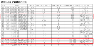
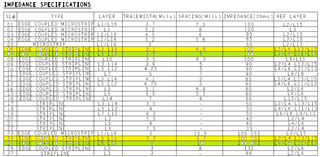
  1. We found a mismatch in the stack-up file (PROC141_STACKUP) & Fab drawing (PROC141E3_FAB) related to impedance & finished copper thickness. Below image for your reference purpose

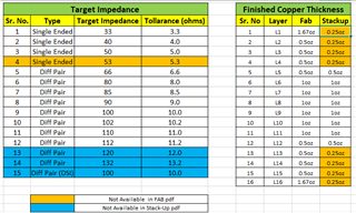
  2. We found 132E impedance in the fab drawing but we are not able to find the same in the schematic. Please let us know for which application we are using 132E impedance.
  • The LPDDR4 CLK should be routed at approx 70-ohm differential impedance.  The CLK signals 'branch' at the memory device (connect two different end-points).  In effort minimize the signal integrity impact - the trace impedance of the 'branch' segments should be double the impedance of the source trace.  However - this impedance often cannot be achieved, so best effort should be done.  Note these trace segments are VERY short.  

  • Hi, Robert, We are still confused about the inconsistency between stack-up file (PROC141_STACKUP) & Fab drawing (PROC141E3_FAB). Can you please confirm which is the correct file to follow?

    Also, from the fab drawing, there is 132E impedance, but could you please confirm which signal is using that impedance?

  • 132E cannot be achieved on the PCB without exceeding the minimum trace width.  Similar with 120E.  There is nothing specifically targeting 53E.  For the remaining item (100E for DSI)....what is different between line 9 and line 15 in your table?

  • Hi Robert,
    We found a mismatch in trace width & clearance for 100E & 100E DSI differential routing on the same layer (L3, L14 & L5, L12) as highlighted below PROC141E3_FAB file. Can you please confirm the same?

  • Both fab drawing (snap-shot you provided) and stack-up show trace width of 3.1mils.  No difference.

    The method of providing the spacing between the traces is different.  The fab drawing shows the spacing (or air-gap) between the traces (edge-to-edge).  This is 6.5mils.  The stack-up shows trace pitch - which is center of trace to center of trace (9.6mils).  So the air-gap between the traces is pitch - trace width...or 9.6-3.1 = 6.5mils.  No difference.

  • Hi Robert,

    We found a mismatch in trace width & clearance in the Fab drawing for 100E & 100E DSI differential routing. We are not comparing Fab drawing & stack up.

    If you check the above yellow highlighted details for 100E impedance it shows 3.1mil trace width & 6.5mil spacing on the L3 & L14 layers. Whereas for 100E DSI impedance, it shows 3.3mil trace width & 9.7mil spacing on the L3 & L14 layers with the same reference layer.

    Same for Hreen highlighted details for 100E impedance it shows 3.5mil trace width & 5mil spacing on the L3 & L14 layers. Whereas for 100E DSI impedance, it shows 4mil trace width & 10mil spacing on the L3 & L14 layers with the same reference layer.

    We want confirmation on the same.

  • The design has two different 100E differential impedance requirements.

    100E Differential Impedance

    100E Differential + 50E Single Impedance.  MIPI D-PHY (CSI, DSI) requires both 100E differential and 50E single ended.

    Does that answer question about why 2 different 100E implementations?

  • Hi Robert,

    Thanks for your clarification...!
    It will help us while creating the PCB stack-up