This thread has been locked.

If you have a related question, please click the "Ask a related question" button in the top right corner. The newly created question will be automatically linked to this question.

EMIF16 Document

a.

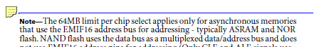
p1-2: Since each CS has 64MB, why cannot NOR flash support 64MB? Instead, it supports 16MB.

Explanation: due to the address line for EMIF which are 24 address lines, hence it can only address up to 16M of location. Each location has 2 bytes. Hence the c66 datasheet is also wrong in saying that it supports 16MB. It should be 16M of location or 32MB.

b.

Since each CS can support up to 16M of location of NOR flash, then the whole device should support up to 16*4=64M of location or 128MB of NOR flash.

Explanation: Only CS4 or CE2 can be used for NOR flash. p25 of c66 datasheet.

c.

p2-5: What is the meaning of address selects in "EMIF[23:22] behave as address selects"? Why for 16bits, EMIFA23 maps to A0 and for 8bits, EMIF23 and 22 map to A1 and A0?

Explanation: ?

d.

p2-5: Is EMIFRnW being used in NOR flash? It is not on the block diagram in p2-4 and p2-5?

Explanation: ?

e.

p2-8: Is EMIFRnW an active high or active low signal? If active high, them the statement "EMIFRnW becomes active (LOW)" should be changed to "becomes inactive".

f.

There seems to be something wrong with the Read and Write diagram Fig2-4 to 2-9. Fig 2-6 and 2-7 is for Select Strobe mode whereas Fig 2-8 and 2-9 is for WE mode. Fig 2-4 and 2-5 is for which mode? Fig2-4 the EMIFBE# is always low, is that correct? Fig2-6, the EMIFBE# seems weird. Fig2-8, the EMIFBE seems weird. 

g. 

Why is that 2 modes - WE and SS? Is it due to different read and write timing diagram of different nor flash memory device? At any one time, the C66 needs to be in in any of the 2 modes? Can it be neither of the 2 modes?


  • Other questions:

    P3-2: NAND Flash mode also supports both 1-bit and 4-bit ECC calculation but 1-2 says it does not support error correction? I believe p1-2 is wrong.

    P3-3: c66 only supports up to 256 MB NAND flash. Is it due to the memory map of c66 datasheet? 1 CS can support 64MB, therefore 4 CS can support 256MB. If that is the case, then if I use up the 4 CS for NAND flash, means that I cannot use for NOR flash. Therefore, the claim by the datasheet that c66 can support 16MB NOR flash and 256MB NAND flash is wrong. It should be 2 options: up to 16MB of NOR and 192MB NAND (Option 1) or up to 256MB NAND flash (option2)

    P3-4: “If using EMIFA11 and EMIFA12 as ALE and CLE respectively” sounds like we can choose other pins as ALE and CLE. Is that correct?

    P2-12: There seems to be very little description for WE mode as compared to SS mode.

    Can help to confirm my understanding for any of the points above. Thanks.

  • Wenjun Huang said:
    b. Since each CS can support up to 16M of location of NOR flash, then the whole device should support up to 16*4=64M of location or 128MB of NOR flash.

    Explanation: Only CS4 or CE2 can be used for NOR flash. p25 of c66 datasheet

    This is incorrect. The datasheet will be updated to show that all 4 CS spaces can be used for NOR. Each will have the same limitation on the size of the NOR Flash for each CS space.

    Wenjun Huang said:
    c. p2-5: What is the meaning of address selects in "EMIFA[23:22] behave as address selects"? Why for 16bits, EMIFA23 maps to A0 and for 8bits, EMIFA23 and 22 map to A1 and A0?

    EMIFA[0] is the 32-bit word address bit. If your physical connection is 8-bits or 16-bits wide, then you need more address bits to select the half-word or byte within the address range that EMIFA[0] can select. This could have been implemented differently, but if you make the connections as shown you will get the functionality that is documented.

    Wenjun Huang said:
    d. p2-5: Is EMIFRnW being used in NOR flash? It is not on the block diagram in p2-4 and p2-5?

    If it is not shown, it is not needed. To what pin on your NOR Flash would you want to connect EMIFRnW?

    Wenjun Huang said:
    e. p2-8: Is EMIFRnW an active high or active low signal? If active high, them the statement "EMIFRnW becomes active (LOW)" should be changed to "becomes inactive".

    Neither. You can see in the Figures that EMIFRnW = 1 during a read operation and = 0 during a write operation. That is its function. Our wording in the document is how the engineer who wrote it considers it to be used in that situation. I do not like the name RnW because the n modifies the W and should therefore be after the W, but this is how it has been forever and I do not expect it to change. Now I understand what the words mean and that is good enough to let me continue working.

    Wenjun Huang said:
    f. There seems to be something wrong with the Read and Write diagrams Fig2-4 to 2-9. Fig 2-6 and 2-7 are for Select Strobe mode whereas Fig 2-8 and 2-9 are for WE mode. Fig 2-4 and 2-5 are for which mode? Fig2-4 the EMIFBE# is always low, is that correct? Fig2-6, the EMIFBE# seems weird. Fig2-8, the EMIFBE seems weird.

    Figures 2-4 and 2-5 give an introduction to the general operation of the EMIF16 in its Normal Asynchronous mode. The Normal Async mode is how it will operate on CS2-4 unless Select Strobe mode is selected. After you understand the concept of how the signals are intended to work in the Normal Async mode, the subsequent sections explain in more detail how the specific SS and WE modes work. CS5 will operate in WE mode unless SS mode is selected; CS5 cannot be configured to operate in Normal Async mode; CS2-4 cannot be configured to operate in WE mode. [ed - RandyP 8/30/2011]

    It appears that the EMIF16 will read all bytes during a read operation. Figures 2-4 and 2-6 show this, but Figure 2-9 shows the lines being high and that is probably an error. Figure 2-8 is for WE mode asynchronous writes; is that why it looks weird to you?

    Wenjun Huang said:
    g. Why is that 2 modes - WE and SS?

    Two modes provide flexibility required for different devices. If one mode fits your device, then you will use that mode.

    Wenjun Huang said:
    P3-2: NAND Flash mode also supports both 1-bit and 4-bit ECC calculation but 1-2 says it does not support error correction? I believe p1-2 is wrong.

    p1-2 is correct. The ECC is calculated. The EMIF16 does not perform error correction, which would mean modifying the data.

    Wenjun Huang said:
    P3-3: c66 only supports up to 256 MB NAND flash.

    We have discussed this before. You need to study the operation of NAND flash devices to understand that the address range of the EMIF does not dictate the accessible size of the NAND Flash.

    Wenjun Huang said:
    P3-4: “If using EMIFA11 and EMIFA12 as ALE and CLE respectively” sounds like we can choose other pins as ALE and CLE. Is that correct?

    If you want to minimize your risk and allow us to provide useful support, implement this the way that we document it to be done. We can tell you a method that works and you can succeed using that method.

    Regards,
    RandyP


    If you need more help, please reply back. If this answers the question, please click  Verify Answer  , below.

  • To add to Randy's very nicely detailed replies, the 64MB per chip select and 256MB across all 4 chip selects needs to be revised.

    Because of the way the EMIF16 controller is designed, we will support a max of 32MB per chip select for NOR flash and SRAM for 16-bit devices and 16MB per chip select for NOR and SRAM for 8-bit devices.

    This limitation does not apply to NAND flash since it does not use EMIF16's address bus for addressing. Rather, it uses the data bus as a multiplexed data/address bus. Hence, NAND flash > 32MB can be supported.

    We are currently working our way with revisions to the data sheet and user guide. The next revisions will clarify this requirement.

  • I downloaded the latest documentation for the C6657 and still got the EMIF16 documentation which states 64MB support per chip select.

    Is the limitation to 32 MB for 16-bit devices an official statement?

  • Manfred,

    Which documentation are you referring to?

    The datasheet says that the four CS ranges are 64MB wide, which is true based on where each one begins. But this is not the same as saying that they support 64MB of accessible memory locations. Please see the Note 1 at the end of the Memory Map Summary for a detailed list of the supported sizes for different memory types.

    Regards,
    RandyP

  • Hello RandyP,

    Thank you for the information where the statement about the limitation of supported NOR flash is found.
    I did search this information in the EMIF16 document and at the chapter "Peripheral Information and Electrical Specifications" for the EMIF16 interface at the datasheet. I didn't search in the footnote of the memory map summary.

    The EMIF16 document states in the chapter "Features" as follows:

    This statement is quite misleading and there is no information in this document that these 64MB can not be physically addressed to the asynchronous memories with the 16bit EMIF interface. I would have preferred that also the EMIF16 document would have been also reworked as Aditya has quoted in this discussion.

    Thanks
    Manfred