Other Parts Discussed in Thread: TDA4VM
Hi there
Hope you are doing well.
I have configured the MCSPI for the following configurations:
- MOA enabled
- master mode
- Single channel enabled for communication
- FORCE: 1
- TURBO: 1
- FIFO enabled for TX only
- TRM: Transmit Mode only
- WL: 7
- SPI Frequency: 50MHz
- Clock divisor: 4096
Questions:
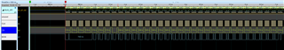
- If TXFFE is empty I am sending 64 bytes to TX FIFO (using TX register, 16 sets of 4 bytes). How will I get to know that 64 bytes have been sent to TX FIFO? Which Flag do I have to check for this case?
Expected Used case:
When TXFEE is empty, I want to transmit 64 bytes of data to TX FIFO (using TX register, 16 sets of 4 bytes) continuously in a while loop and want to exit the function. In the meantime, shift registers will transmit
the data from TX FIFO to the slave connected. If I want to transmit the data again to TX FIFO if TXFEE is not empty, I want to see device is busy (or shift registers are busy).
Issue faced:
The data received from TX FIFO to the connected slave is corrupted. I can only see the 1 data byte and last data byte (64th byte) to the slave connected.
How to make sure the data from the TX FIFO is correctly received at the connected slave. Which flags to check to make sure the uncorrupted transmission of the data ? - What does EOT signifies in CH_STAT register? Is it 1 when the TX register unload the 4Bytes data at TX FIFO or When the next set of data id loaded on TX register ?
- In MCSPI_IRQSTATUS register filed TX0_EMPTY, the description says Transmit register empty. Also in MCSPI_CHSTAT_0 Register field TXS, the description says channel transmit register. What is he difference between these transmit register ? Which flag is raised when ?
I already go through the TRM, it will be great if you can provide additional information.
Looking forward to hearing back from you.
Best regards,
Hasan