This thread has been locked.

If you have a related question, please click the "Ask a related question" button in the top right corner. The newly created question will be automatically linked to this question.

TDA4VM-Q1: TDA4VM DDR eye diagram test issue

Part Number: TDA4VM-Q1
Other Parts Discussed in Thread: TDA4VM,

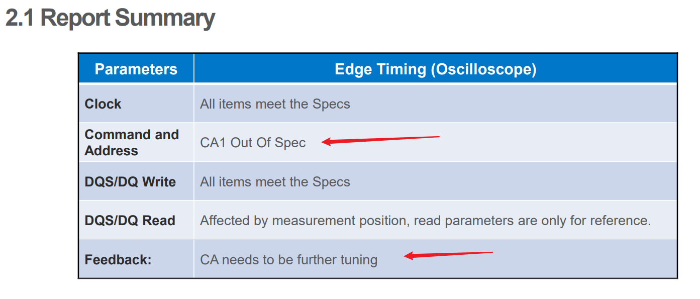
We tested DDR DQ write eye Diagram failed (as shown in Figure 1 below) on the board of TDA4VM with Micron MT53E512M32D1ZW-046 AUT:B in D (short name ) project. Comparing the fine eye map of the previous L project which TDA4VM with MT53E1G32D2FW-046 AAT:A (as shown in Figure 2 below), I find that the main cause is that the center point of DQS is not in the middle of the eye of DQ write. The D project SPRACU8B_Jacinto7_DDRSS_RegConfigTool value olso checked OK by Micron FAE.

Our other project H, also had the same problem.The H project is TDA4VM with MT53E1G32D2FW-046 AAT:B
Today, I change the MT53E1G32D2FW-046 AAT:A to the D project board ,use the same D project software test the DDR DQ write eye Diagram is passed(as shown in Figure 3 below), so I confused, same software,same PCB,different LPDDR4 part number,only with MT53E1G32D2FW-046 AAT:A DDR can pass the DDR DQ write eye Diagram.
please help improve DDR DQ write eye Diagram on the D project ,which is TDA4VM with Micron MT53E512M32D1ZW-046 AUT:B
When we tested the eye Diagram, we turned off the DQ training function as recommended by E2E to prevent thin lines from passing through the middle of the eye. Here is a link to how to turn off DQ training.TDA4VM-Q1: TDA4VM-Q1 - Processors forum - Processors - TI E2E support forums

  • Hello,

    We are reassigning this to the DDR expert. Please allow our team a day or two to look at your query and respond.

    Thanks.

  • Thank you !

    I attatched the three projects DDRSS Regconfig tool parameters

    SPRACU8_Jacinto7_DDRSS_RegConfigTool-sampleA-2133_L project.xlsm

  • Hi,

    I want to upload a 2MB size file , but failed , how to do that ?

  • Hi,

    Are you observing functional failures (system crashing / etc.) , or is the concern just isolated to the waveform measurements?

    Can you load the attached binary to the R5 core through Code Composer Studio, execute the code, and provide the output?

    8306.tda4x_lp4_debug.zip

    Regards,
    Kevin

  • Hi, Kevin

    I am software colleague of Pengpeng.

    Are you observing functional failures (system crashing / etc.) , or is the concern just isolated to the waveform measurements?

    No functional failures, system is running normally.
    It is the concern just isolated to the waveform measurements.

    Can you load the attached binary to the R5 core through Code Composer Studio, execute the code, and provide the output?

    1. We do not have experience with Code Composer Studio. Could you please provide a program binary that can be run from an SD card or OSPI Flash?
    2. What does the 'output' specifically refer to, is it a UART log?

    Thank you.

    BRs

  • Hi,

    No functional failures, system is running normally.
    It is the concern just isolated to the waveform measurements.

    Thanks - my concern is that this isn't a real failure, and just an artifact of the waveform measurement. In the failure plot, the DQ is almost switching at the same time as the DQS crossing. If real, I would assume this would likely lead to functional failures.

    The LPDDR4 uses an un-matched DQS to DQ path and there is an offset of tDQS2DQ. How does this get accounted for in the measurements?

    We do not have experience with Code Composer Studio

    We have a software tool that could capture the eye opening which might be a better tool to run instead of the previous binary I provided. However, it also requires CCS. We can give basic instructions on how to create a target configuration file / load & execute a pre-built binary, but that may not be worthwhile if you do not have JTAG access or an emulator. Do your custom boards have JTAG access? Do you have any emulator? 

    Regards,
    Kevin

  • Hi Kevin
    Thank you for your reply.

    The LPDDR4 uses an un-matched DQS to DQ path and there is an offset of tDQS2DQ. How does this get accounted for in the measurements?

    We are confirming with the LPDDR4 manufacturer.

    We have a software tool that could capture the eye opening which might be a better tool to run instead of the previous binary I provided. However, it also requires CCS. We can give basic instructions on how to create a target configuration file / load & execute a pre-built binary, but that may not be worthwhile if you do not have JTAG access or an emulator. Do your custom boards have JTAG access? Do you have any emulator? 

    Thank you.
    Our custom board have JTAG access, and we have a XDS560 emulator.
    I tried load tda4vm_lp4_debug.out and run on MCU1_0 R5 core through Code Composer Studio.
    I run it three times, the output of the three times as follows:

    ccs_output.zip


    My steps to run tda4vm_lp4_debug.out:
    1、Boot our custom board from SD Card, HLOS is Linux.
    2、Launch the target config file.
        The target config created according to 6.4. Debugging with HLOS running on A72
        https://software-dl.ti.com/jacinto7/esd/processor-sdk-rtos-jacinto7/08_04_00_06/exports/docs/psdk_rtos/docs/user_guide/ccs_setup_j721e.html
    3、Connect to the MCU1_0 R5 Core, load tda4vm_lp4_debug.out binary and run.
    4、CCS console output come up.


    Could you please check if my step is correct and provide basic instructions on how to create a target configuration file / load & execute a pre-built binary?

    BRs

  • Hi Tiancheng

    Could you please check if my step is correct and provide basic instructions on how to create a target configuration file / load & execute a pre-built binary?

    Yes, your step is correct.

    I run it three times, the output of the three times as follows:

    ccs_output.zip

    From your log, there is only a max PLL timeout which can be eliminated with using v0.10.0 tool and should be not related to this issue. Kevin, could you please help to double check? Thanks

  • The LPDDR4 uses an un-matched DQS to DQ path and there is an offset of tDQS2DQ. How does this get accounted for in the measurements?

    Attached is the DDR SI report tested by Micron for us, which indicates that the tCIVW-R time of CA1 exceeds the standard. Is there any way for TI to optimize this time parameter? By the way, during the Micron test, DDR interposer  was welded twice before it was successfully boot. They believed that it was the abnormality of TCIVW-R of CA1 that caused the first welding to fail to start normally.Eye maps testing DQS and DQ in the report found no problems,however in my opinion, tDQS2DQ this time parameter should be close to the integer multiple of 0.5UI is the best.It should be noted that this parameter is close to 0.5UI in the fully pass report of other projects tested in the past.

    In addition, Micron Laboratory helped us to do a cross test, programed other project software versions that could pass the DDR test  onto this problematic board, and the tCIVW of the test CA1 was changed to abnormal on the left side. The test results are shown in the figure below.And the CS0 is OK.