This thread has been locked.

If you have a related question, please click the "Ask a related question" button in the top right corner. The newly created question will be automatically linked to this question.

TDA4VM: Togging TP100 (GPIO0_52) on j721excp01evm

Part Number: TDA4VM

Hello,

Following your instructions Iam able to toggle TP_45 (GPIO0_6). 

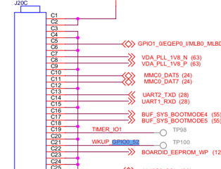
I want to do the same for TP100 (GPIO0_52), but I can not see any toggle.

I have doubts if registers I am using are correct, also bit fields. Please let me know. 

1. Select a GPIO that has TP attached to it (You could refer the SCH and ASSY file of the board)
-> WKUP_GPIO0_52 connected to TP100

2. Get the ballnumber of the GPIO selected from the datasheet from section 6.2 Pin Attributes.
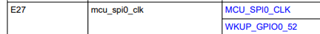
-->Ball E27


3. Identify the padconfig register address for the particular GPIO using the datasheet from section 6.4 Pin Multiplexing.
--> PADCONFIG 36 for ballnumber E27

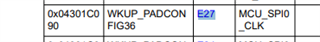
4. Identify the Kick register from the padconfig register address obtained above TRM section 5.1 Control Module
-->  
Eg. padconfig 50 = 0x4301C090 (offset 1C090) so select LOCK7_KICK0 register address


5. Identify the GPIO Bank from the GPIO number from TRM Section 12.1.2 GPIO
   Here I have doubts, should it be Bank3?

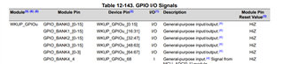
6. Get the DIR and OUT_DATA register offset w.r.t the gpio bank selected

   Here I have doubts, should it be Bank3?

Then bit to be changed values to togle will be

*outData23 &= 0xFFDFFFFF;

*outData23 |= 0x00200000;

Using

#define WKUP_2_PADCONFIG 36 /*GPIO0_52, TP100, Ball E27*/

uint32_t * padconfig2 = (uint32_t *) WKUP_2_PADCONFIG;

volatile uint32_t * dir23 = (uint32_t *) 0x42110038;

volatile uint32_t * outData23 = (uint32_t *) 0x4211003C;

BR

  • Hi

    Here I have doubts, should it be Bank3?

    Yes, Correct.

    Could you try this?

    #define WKUP_PADCONFIG     36
    
    #define M4_PINMUX_VALUE(_rxActive, _pullType, _pull, _mux)  ((_rxActive << 18) | (_pullType << 17) | (_pull << 16) | (_mux << 0))
    
    #define M4_WKUP_PADCONFIG   0x4301C000
    
    #define M4_RX_ACTIVE        1
    #define M4_RX_INACTIVE      0
    
    #define M4_PULL_DOWN        0
    #define M4_PULL_UP          1
    
    #define M4_PULL_ENABLED     0
    #define M4_PULL_DISABLED    1
    
    #define M4_MUX_MODE_0   0x0
    #define M4_MUX_MODE_1   0x1
    #define M4_MUX_MODE_7   0x7   // ---> MUX MODE 7 to configure the PIN as GPIO
    
    volatile uint32_t *LOCK7_KICK0  = (uint32_t *) 0x4301d008;
    uint32_t * padconfig = (uint32_t *) M4_WKUP_PADCONFIG;
    volatile uint32_t * dir01 = (uint32_t *) 0x42110038;
    volatile uint32_t * outData01 = (uint32_t *) 0x4211003C;
    
    
    inside the function
    {
    
        //unlock ctrl mmr
        LOCK7_KICK0[0] = 0x68EF3490;
        LOCK7_KICK0[1] = 0xD172BC5A;
    
        // configure GPIO pad, write to ctrl mmr
        padconfig[WKUP_PADCONFIG] = M4_PINMUX_VALUE(M4_RX_INACTIVE, M4_PULL_UP, M4_PULL_DISABLED, M4_MUX_MODE_7);
    
        // set as output
        *dir01 &= 0x0000ffff; 
    	
        // drive low
        *outData01 &= 0x0000ffff; 
    
        //Delay (You could use your own way to add delay)
        appLogWaitMsecs(1000); 
     
        // drive high
        *outData01 |= 0xffff0000; 
    
    }

    Regards,

    Nikhil

  • Hello

    The proposed code crashes the system. I guess is becasue we are changing 16 signals that are input to output instead just the one I want, GPIO0_52. I should check what are connected to those other signals that are set as output and the influence to cause this crashing.

  • Hi Pablo,

    Let me try this at my end and i shall update you with results next week and I'm currently on travel.

    Regards,

    Nikhil

  • Hello Nikhil.

    I have resolved the issue.

    I was toggling wrong bit. Because of that, I was changing GPIO0_53 and system was like crashed. Your solution did also that (in fact it was toggling all 16 GPIOs on bank3)

    Just for information to whom can interest: GPIO0_53 is managing System Power Down !

    Finally, toggling must be done in this way:

    *outData23 &= ~( 1U << 20U); /* GPIO number minus number of completed banks (0 & 1): 52 -32*/
    
    *outData23 |= ( 1U << 20U);

    BR

  • Hi Pablo,

    Thank you for this info. and confirmation.

    Regards,

    Nikhil