This thread has been locked.

If you have a related question, please click the "Ask a related question" button in the top right corner. The newly created question will be automatically linked to this question.

TDA4VM: R5 MPU Config break after switch from PSDKR v09_00 to v09_01

Part Number: TDA4VM

Hi Ti,

after PSDK RTOS Update from v09_00 to v09_01 all our R5 applications did not work anymore.

More specific, the R5 cores entered "prefetch exception" state after configuring and activating MPU unit.

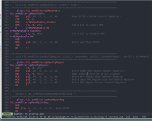
After rereading documentation, and poking around source-code this changeset grabbed my attention:

Left is v09_00, right is v09_01: pdk_jacinto*/packages/ti/csl/arch/r5/startup.c

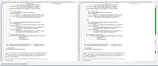
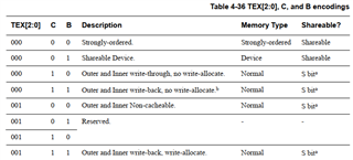
Line 150, 153 on right side: accessCtrlRegVal is set differently. gMemAttr did not change, so for me it seems quite obvious that existing MPU-Configurations will break.

Could you explain please that change? And why is that not documented?

Thank you, and best regards,
Thomas

  • Hi Thomas,

    Thanks for pointing this out. Does it work fine if you revert this change? C and B attribute decides the memory type, so potentially can have effect. Can you please try reverting it?

    Regards,

    Brijesh

  • Hi Brijesh,

    yes. It works fine when I revert that particular change.

    Regards,
    Thomas

  • Hi Thomas,

    According to the below comment in the code, it seems the change is correct. Have you also updated/added new MPU region in your codebase?  

    /* Declarations */
    /**
    * \brief TEX[2:0], C and B values.
    * CSL_ArmR5MemAttr is used as intex here.
    * gMemAttr[x][0]: TEX[2:0] values
    * gMemAttr[x][1]: C bit value
    * gMemAttr[x][2]: B bit value
    * Note: memAttr field is valid only if cacheable = FALSE.
    * For more details, refer #CSL_ArmR5MpuRegionCfg
    */
    const uint32_t gMemAttr[CSL_ARM_R5_MEM_ATTR_MAX][3U] __attribute__((section(".startupData"))) =
    {
    /* TEX[2:0], C, B bits */

    In vision apps application, we always use memAttr as 0, which means C and B bits were always 0, so it was working fine, ever after this change. 

    So wanted to understand if you have added any region with the different memAttr? 

    Regards,

    Brijesh

  • Hi Brijesh,

    yes, we have added MPU region in our codebase which differs from the vision apps.

    As an example:

    {
          /* Region 6 configuration: 512 KB MAIN MSRAM */
          /* Used for:
          * MAIN_IC_MPU_MCU2_0_ADDR
          * MAIN_IC_MCU2_0_MCU2_1_ADDR
          * MAIN_IC_READ_SMALL_FROM_EP_ADDR
           * */
         .regionId         = 6U,
         .enable           = 1U,
         .baseAddr         = 0x3600000,
         .size             = CSL_ARM_R5_MPU_REGION_SIZE_512KB,
         .subRegionEnable  = CSL_ARM_R5_MPU_SUB_REGION_ENABLE_ALL,
         .exeNeverControl  = 0U,
         .accessPermission = CSL_ARM_R5_ACC_PERM_PRIV_USR_RD_WR,
         .shareable        = 0U,
         .cacheable        = (uint32_t)FALSE,
         .cachePolicy      = 0U,
         .memAttr          = CSL_ARM_R5_MEM_ATTR_CACHED_WT_NO_WA,
     },
    
     {
          /* Region 7 configuration: Memory for communication between MCU2_0 and Linux via DMA [ size  8.00 MB ] */
         .regionId         = 7U,
         .enable           = 1U,
         .baseAddr         = DDR_MCU2_0_MPU_ADDR,
         .size             = CSL_ARM_R5_MPU_REGION_SIZE_8MB,
         .subRegionEnable  = CSL_ARM_R5_MPU_SUB_REGION_ENABLE_ALL,
         .exeNeverControl  = 0U,
         .accessPermission = CSL_ARM_R5_ACC_PERM_PRIV_USR_RD_WR,
         .shareable        = 0U,
         .cacheable        = (uint32_t)FALSE,
         .cachePolicy      = 0U,
         .memAttr          = CSL_ARM_R5_MEM_ATTR_SHAREABLE,
     },
    
     {
          /* Region 8 configuration: MCU Interconnect for commununcation between MCU2_0 and MCU1_0 [ size 16.00 KB ] */
         .regionId         = 8U,
         .enable           = 1U,
         .baseAddr         = MCU_IC_MCU2_0_MCU1_0_ADDR,
         .size             = CSL_ARM_R5_MPU_REGION_SIZE_16KB,
         .subRegionEnable  = CSL_ARM_R5_MPU_SUB_REGION_ENABLE_ALL,
         .exeNeverControl  = 0U,
         .accessPermission = CSL_ARM_R5_ACC_PERM_PRIV_USR_RD_WR,
         .shareable        = 0U,
         .cacheable        = (uint32_t)FALSE,
         .cachePolicy      = 0U,
         .memAttr          = CSL_ARM_R5_MEM_ATTR_SHAREABLE,
     },

    I would like to know, which PSDKR version is correct in that regard and if that will be changed again (silently) in future releases?

    Regards,
    Thomas

  • Hi Thomas,

    As per the below table from R5F specs, 

    the code below is setting up these bits correctly now in the SDK9.1 release. In your code, you are using index 1 and index 2, as highlighted below. That's exactly matching with the above table now. 

    /* Declarations */
    /**
    * \brief TEX[2:0], C and B values.
    * CSL_ArmR5MemAttr is used as intex here.
    * gMemAttr[x][0]: TEX[2:0] values
    * gMemAttr[x][1]: C bit value
    * gMemAttr[x][2]: B bit value
    * Note: memAttr field is valid only if cacheable = FALSE.
    * For more details, refer #CSL_ArmR5MpuRegionCfg
    */
    const uint32_t gMemAttr[CSL_ARM_R5_MEM_ATTR_MAX][3U] __attribute__((section(".startupData"))) =
    {
    /* TEX[2:0], C, B bits */
    { 0x0U, 0x0U, 0x0U,}, /* Strongly-ordered.*/
    { 0x0U, 0x0U, 0x1U,}, /* Shareable Device.*/
    { 0x0U, 0x1U, 0x0U,}, /* Outer and Inner write-through, no write-allocate. */
    { 0x0U, 0x1U, 0x1U,}, /* Outer and Inner write-back, no write-allocate. */
    { 0x1U, 0x0U, 0x0U,}, /* Outer and Inner Non-cacheable. */
    { 0x1U, 0x1U, 0x1U,}, /* Outer and Inner write-back, write-allocate.*/
    { 0x2U, 0x0U, 0x0U,}, /* Non-shareable Device.*/
    };

    Regards

    Brijesh

  • Thank you Brijesh for clarifying this.

    It is a bit odd, that somehow our MPU Configuration let the R5 crash - even it should now set the TEX,C,B correct with SDK9.1

    Here is the full MPU Config from our R5-Example which works on SDK9.0 and fails with SDK9.1:

    /*Note: cacheable should always be set to FALSE.
     * The naming is misleading, since all settings you can set using cacheable, can also be set via memAttr.
     * If cacheable is set to FALSE, entries in cachePolicy are ignored.
     *
     * CSL_ARM_R5_MEM_ATTR_SHAREABLE enables the cache line of R5. That means, 32 Byte are read/written at once.
     * NO "ATOMIC" 4 Byte access!!! So be careful.
     * The additional SHAREABLE flag, indicates if the caches are actual active. If yes, manual flush/invalidate
     * may required in programmers code.
    */
    
    const CSL_ArmR5MpuRegionCfg  gCslR5MpuCfg[CSL_ARM_R5F_MPU_REGIONS_MAX] =
    {
        {
                /* Region 0 configuration: complete 32 bit address space = 4Gbits
                 * Enable 4 Byte Access via CSL_ARM_R5_MEM_ATTR_CACHED_WT_NO_WA (because of peripherals) */
                .regionId         = 0U,
                .enable           = 1U,
                .baseAddr         = 0x0U,
                .size             = CSL_ARM_R5_MPU_REGION_SIZE_4GB,
                .subRegionEnable  = CSL_ARM_R5_MPU_SUB_REGION_ENABLE_ALL,
                .exeNeverControl  = 1U,
                .accessPermission = CSL_ARM_R5_ACC_PERM_PRIV_USR_RD_WR,
                .shareable        = 1U,
                .cacheable        = (uint32_t) FALSE,
                .cachePolicy      = 0U,
                .memAttr          = CSL_ARM_R5_MEM_ATTR_STRONGLY_ORDERED,
        },
        {
                /* Region 1 configuration: 128 bytes memory for exception vector execution */
                .regionId         = 1U,
                .enable           = 1U,
                .baseAddr         = 0x0U,
                .size             = CSL_ARM_R5_MPU_REGION_SIZE_128B,
                .subRegionEnable  = CSL_ARM_R5_MPU_SUB_REGION_ENABLE_ALL,
                .exeNeverControl  = 0U,
                .accessPermission = CSL_ARM_R5_ACC_PERM_PRIV_USR_RD_WR,
                .shareable        = 0U,
                .cacheable        = (uint32_t)FALSE,
                .cachePolicy      = 0U,
                .memAttr          = CSL_ARM_R5_MEM_ATTR_SHAREABLE,
        },
        {
                /* Region 2 configuration: Disable all access to DDRAM except of the following areas */
                .regionId         = 2U,
                .enable           = 0U,
                .baseAddr         = 0x80000000,
                .size             = CSL_ARM_R5_MPU_REGION_SIZE_4GB,
                .subRegionEnable  = CSL_ARM_R5_MPU_SUB_REGION_ENABLE_ALL,
                .exeNeverControl  = 0U,
                .accessPermission = CSL_ARM_R5_ACC_PERM_PRIV_USR_RD_WR,
                .shareable        = 0U,
                .cacheable        = (uint32_t)FALSE,
                .cachePolicy      = 0U,
                .memAttr          = CSL_ARM_R5_MEM_ATTR_SHAREABLE,
        },
        {
                /* Region 3 configuration: DDR_MCU2_0_IPC +  DDR_MCU2_0_RESOURCE_TABLE + DDR_MCU2_0*/
                .regionId         = 3U,
                .enable           = 1U,
                .baseAddr         = DDR_MCU2_0_IPC_ADDR,
                .size             = CSL_ARM_R5_MPU_REGION_SIZE_8MB,
                .subRegionEnable  = CSL_ARM_R5_MPU_SUB_REGION_ENABLE_ALL,
                .exeNeverControl  = 0U,
                .accessPermission = CSL_ARM_R5_ACC_PERM_PRIV_USR_RD_WR,
                .shareable        = 0U,
                .cacheable        = (uint32_t)FALSE,
                .cachePolicy      = 0U,
                .memAttr          = CSL_ARM_R5_MEM_ATTR_SHAREABLE,
        },
    
        {
                /* Region 4 configuration: 32 KB BTCM */
                /* Address of ATCM/BTCM are configured via MCU_SEC_MMR registers
                   It can either be '0x0' or '0x41010000'. Application/Boot-loader shall
                   take care this configurations and linker command file shall be
                   in sync with this. For either of the above configurations,
                   MPU configurations will not changes as both regions will have same
                   set of permissions in almost all scenarios.
                   Application can chose to overwrite this MPU configuration if needed.
                   The same is true for the region corresponding to ATCM. */
                .regionId         = 4U,
                .enable           = 1U,
                .baseAddr         = 0x41010000,
                .size             = CSL_ARM_R5_MPU_REGION_SIZE_32KB,
                .subRegionEnable  = CSL_ARM_R5_MPU_SUB_REGION_ENABLE_ALL,
                .exeNeverControl  = 0U,
                .accessPermission = CSL_ARM_R5_ACC_PERM_PRIV_USR_RD_WR,
                .shareable        = 0U,
                .cacheable        = (uint32_t)FALSE,
                .cachePolicy      = 0U,
                .memAttr          = CSL_ARM_R5_MEM_ATTR_SHAREABLE,
        },
        {
                /* Region 5 configuration: 32 KB ATCM */
                .regionId         = 5U,
                .enable           = 1U,
                .baseAddr         = 0x0,
                .size             = CSL_ARM_R5_MPU_REGION_SIZE_32KB,
                .subRegionEnable  = CSL_ARM_R5_MPU_SUB_REGION_ENABLE_ALL,
                .exeNeverControl  = 0U,
                .accessPermission = CSL_ARM_R5_ACC_PERM_PRIV_USR_RD_WR,
                .shareable        = 0U,
                .cacheable        = (uint32_t)FALSE,
                .cachePolicy      = 0U,
                .memAttr          = CSL_ARM_R5_MEM_ATTR_SHAREABLE,
        },
    
     {
          /* Region 6 configuration: 512 KB MAIN MSRAM */
          /* Used for:
          * MAIN_IC_MPU_MCU2_0_ADDR
          * MAIN_IC_MCU2_0_MCU2_1_ADDR
          * MAIN_IC_READ_SMALL_FROM_EP_ADDR
           * */
         .regionId         = 6U,
         .enable           = 1U,
         .baseAddr         = 0x3600000,
         .size             = CSL_ARM_R5_MPU_REGION_SIZE_512KB,
         .subRegionEnable  = CSL_ARM_R5_MPU_SUB_REGION_ENABLE_ALL,
         .exeNeverControl  = 0U,
         .accessPermission = CSL_ARM_R5_ACC_PERM_PRIV_USR_RD_WR,
         .shareable        = 0U,
         .cacheable        = (uint32_t)FALSE,
         .cachePolicy      = 0U,
         .memAttr          = CSL_ARM_R5_MEM_ATTR_CACHED_WT_NO_WA,
     },
    
     {
          /* Region 7 configuration: Memory for communication between MCU2_0 and Linux via DMA [ size  8.00 MB ] */
         .regionId         = 7U,
         .enable           = 1U,
         .baseAddr         = DDR_MCU2_0_MPU_ADDR,
         .size             = CSL_ARM_R5_MPU_REGION_SIZE_8MB,
         .subRegionEnable  = CSL_ARM_R5_MPU_SUB_REGION_ENABLE_ALL,
         .exeNeverControl  = 0U,
         .accessPermission = CSL_ARM_R5_ACC_PERM_PRIV_USR_RD_WR,
         .shareable        = 0U,
         .cacheable        = (uint32_t)FALSE,
         .cachePolicy      = 0U,
         .memAttr          = CSL_ARM_R5_MEM_ATTR_SHAREABLE,
     },
    
     {
          /* Region 8 configuration: MCU Interconnect for commununcation between MCU2_0 and MCU1_0 [ size 16.00 KB ] */
         .regionId         = 8U,
         .enable           = 1U,
         .baseAddr         = MCU_IC_MCU2_0_MCU1_0_ADDR,
         .size             = CSL_ARM_R5_MPU_REGION_SIZE_16KB,
         .subRegionEnable  = CSL_ARM_R5_MPU_SUB_REGION_ENABLE_ALL,
         .exeNeverControl  = 0U,
         .accessPermission = CSL_ARM_R5_ACC_PERM_PRIV_USR_RD_WR,
         .shareable        = 0U,
         .cacheable        = (uint32_t)FALSE,
         .cachePolicy      = 0U,
         .memAttr          = CSL_ARM_R5_MEM_ATTR_SHAREABLE,
     },
    {
        /* Region 9 configuration: APP_LOG_MEM which needs to be uncached for proper function [ size 256.00 KB ] */
        .regionId         = 9U,
        .enable           = 1U,
        .baseAddr         = APP_LOG_MEM_ADDR, // 0xAD000000u,
        .size             = CSL_ARM_R5_MPU_REGION_SIZE_256KB,
        .subRegionEnable  = CSL_ARM_R5_MPU_SUB_REGION_ENABLE_ALL,
        .exeNeverControl  = 0U,
        .accessPermission = CSL_ARM_R5_ACC_PERM_PRIV_USR_RD_WR,
        .shareable        = 0U,
        .cacheable        = (uint32_t)FALSE,
        .cachePolicy      = 0U,
        .memAttr          = CSL_ARM_R5_MEM_ATTR_CACHED_WT_NO_WA,
    },
    
    };

    Do you notice any inconstancy here?

    Regards,
    Thomas

  • Hi Thomas,

    Looking at the region settings, it looks to be fine. Is it possible to know exactly where it crashes with prefetch abort issue? 

    What i am thinking is, the above change interchanges device memory with normal memory (write through) and if there is any access to device, may be out of order, then can potentially cause abort. But we need to see where exactly it crashes. 

    Regards,

    Brijesh

  • Hi Brijesh,

    yes. The prefetch abort issue happens exactly when line 160 of pdk_jacinto_09_01_00_22/packages/ti/csl/arch/r5/src/startup/r5_startup.asm gets executed.

    From my point of view, following happens in summary:

    1. R5 out of reset.
    2. MPU gets configured
    2.1 MPU gets disabled
    2.2 MPU Config Array gets applied
    2.3 MPU gets enabled

    At step 2.3, when armR5MpuEnable_00 is executed, there is first a Data Synchronisation Barrier (DSB), then SCTLR gets modified (enable MPU), then Instruction Synchronisation Barrier (ISB).

    After ISB, the R5 jumps to prefetch abort exception state.

    I can also sent you the ELF file with debug symbols if that helps here.

    Regards,

    Thomas

  • Hi Thomas,

    Not sure exactly why this pre-fetch abort happens, we will have to try it out to see on EVM.

    In your MPU configuration file, can you interchange CSL_ARM_R5_MEM_ATTR_SHAREABLE and CSL_ARM_R5_MEM_ATTR_CACHED_WT_NO_WA to fix this issue?  

    Regards,

    Brijesh

  • Hi Brijesh,

    sorry for the delay, I wasn't in the office the last couple of days.

    So, the interchange worked, our apps are working again. However it is still a bit confusing to me, why the prefetch exception happens. Maybe the interchange of memory type (normal/device memory) could be the issue here?

    It would be nice to know what actually triggered the prefetch exception.

    Thank you and best regards,
    Thomas

  • Hi Thomas,

    ok, i am also suspecting memory type, but will need to try it out and see exact reason for abort. 

    Regards,

    Brijesh

  • Hi Thomas,

    I will this ticket open, but lower priority, because we already have solution for it. Hope this is ok.

    Regards,

    Brijesh

  • Hi Brijesh,

    yes it's okay.

    Regards,

    Thomas