This thread has been locked.

If you have a related question, please click the "Ask a related question" button in the top right corner. The newly created question will be automatically linked to this question.

DRA829J: PLL Programming Requirements

Part Number: DRA829J

Dear Ti-Team,

we're currently working on PLL configuration routine (without DMSC due to our project restrictions) and faced some difficulties.

Could you please clarify the following questions:

  • Acc. to the TRM (SPRUIL1C) chapter "5.4.5.10.1.3" a PLL VCO must be >1500MHz (see below), but it contradicts to the TI default configuration:


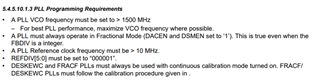
    Q1: Is this requirement regarding minimal PLL VCO valid or not?

  • According with the TRM, DSMEN and DACEN fields of PLL CTRL register have to be always set:


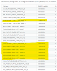
    Documentation suggests PLL type must always operate in fractional mode which makes sense as DACEN and DSMEN are enabled, however, TI default values have DSMEN cleared for the MCU_PLL0 and PLL0, suggesting they are operating in integer mode.

    Furthermore, MCU_PLL0 and PLL0 have their fractional divider set to 0, which also suggest the clear of DSMEN.

    Q2: Is documentation correct? Should DSMEN and DACEN be set to 1 by default? As far as we understand it, when fractional divider is set to 0, DSMEN should be cleared.

  • We're trying to configure register PLLDIV2 to configure the MCU_SYSCLK0 and MAIN_SYSCLK0 clocks.

    However, we're failing to understand PLLDIV2 functionality. Documentation does not give a lot of details, CTT also seems not having information about it. 

    As far as we understand, if PLLSELB of PLLCTRL value is set to zero, only PLLDIV1 is used and PLLDIV2 is not relevant.

    Q3: Should the PLL Controller register PLLDIV2 be configured? What is its functionality?

  • The following extract from the TRM requires calibration procedure to be done for a PLL:


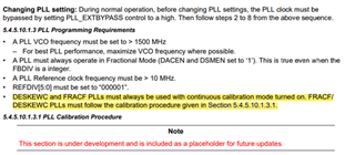
    Calibration procedure is not present in either “B” or “C” revisions of the TRM.

    Q4: What is the correct calibration procedure?

  • Chapter "5.4.5.10.4 Entire Sequence for Programming PLLCTRL, HSDIV, and PLL” of TRM requires to have a delay after specific steps. However delay values are not specified.

    Q5: Which constraints for these delay have to be taken into account while programming PLLs?

  • Chapter "5.4.5.10.4 Entire Sequence for Programming PLLCTRL, HSDIV, and PLL” of TRM contains two steps "Configure PLL dividers" and "Configure "random" PLL controls".

    In this steps some of the settings duplicate each other, e.g. REF_DIV = 1, POST_DIV1 = 1 and POST_DIV2 = 1.

    Q6: Is it really necessary to repeat some settings? Should these two steps be performed in the order defined in the TRM (with doubled settings of some regs)?

    Q7: POST_DIV1 =1 and POST_DIV2 = 1 is not traceable to default TI PLL configuration (not always value 1 is used). Is it a typo? 

Best regards,
Dmitry

  • Hi Dmitry,

    The assigned engineer is looking into this for you. Thank you for your patience.

    Best regards,

    Fabiana

  • Hello Fabiana,

    is there any feedback might be given or are the queries still in work?

    Regards,
    Dmitry

  • Dmitry,

    I am working on your questions. Can you maybe show where you got your table?

    Kevin

  • Hi Kevin,

    if you're about the PLL outputs, it is taken from TISCI documentation (see J721E PLL Defaults — TISCI User Guide) and I think the values are acc. to TI SBL.

    Regards,
    Dmitry

  • Thanks. I don't really know what CLKOUT means....  I have expanded the table to show VCO and divided frequencies:

    HSDIV  freq [MHz]
    PLL VCO 0 1 2 3 4 5 6 7 8
    MAIN (PLLFRACF2_SSMOD_16FFT_MAIN_0) 2000 500 400 200 133.3333 80 100 500 400 500
    PER0 (PLLFRACF2_SSMOD_16FFT_MAIN_1) 1920 192 320 192 192 - 384 38.4 48 40
    PER1 (PLLFRACF2_SSMOD_16FFT_MAIN_2) 1800 - 600 200 300 100 - 225 120 -
    CPSW (PLLFRACF2_SSMOD_16FFT_MAIN_3) 2500 250 250 192.3077 250 156.25 - - - -
    AUDIO (PLLFRACF2_SSMOD_16FFT_MAIN_4) 2359.296 196.608 294.912 196.608 - - - - - -
    VIDEO (PLLFRACF2_SSMOD_16FFT_MAIN_5) 2400 400 600 - - - - - - -
    GPU (PLLFRACF2_SSMOD_16FFT_MAIN_6) 1600 800 - - - - - - - -
    C7X (PLLFRACF2_SSMOD_16FFT_MAIN_7) 2000 1000 - - - - - - - -
    ARM (PLLFRACF2_SSMOD_16FFT_MAIN_8) 2000 2000 - - - - - - - -
    ARM (PLLFRACF2_SSMOD_16FFT_MAIN_9) 2000 2000 - - - - - - - -
    DDR (PLLFRACF2_SSMOD_16FFT_MAIN_12) 2133.33 1066.665 - - - - - - - -
    R5F (PLLFRACF2_SSMOD_16FFT_MAIN_14) 2000 1000 1000 1000 - - - - - -
    DSS (PLLFRACF2_SSMOD_16FFT_MAIN_16) 2970 594 594 - - - - - - -
    DSS (PLLFRACF2_SSMOD_16FFT_MAIN_17) 2970 594 594 - - - - - - -
    DSS (PLLFRACF2_SSMOD_16FFT_MAIN_19) 1800 600 - - - - - - - -
    VISION (PLLFRACF2_SSMOD_16FFT_MAIN_25) 2880 480 720 - - - - - - -
    DDR (PLLFRACF2_SSMOD_16FFT_MAIN_26) 2133.33 1066.665 - - - - - - - -
    DDR (PLLFRACF2_SSMOD_16FFT_MAIN_27) 2133.33 1066.665 - - - - - - - -
    DDR (PLLFRACF2_SSMOD_16FFT_MAIN_28) 2133.33 1066.665 - - - - - - - -
    MCU_PULSAR (PLLFRACF2_SSMOD_16FFT_MCU_0) 2000 1000 58.82353 - - - - - - -
    MCU_PER (PLLFRACF2_SSMOD_16FFT_MCU_1) 2400 400 60 80 96 133.3333 - - - -
    MCU_CPSW (PLLFRACF2_SSMOD_16FFT_MCU_2) 2000 250 500 200 80 166.6667 - - - -

    The point is that the VCO is above 1500 MHz in every case.

    Kevin

  • Hi Kevin,

    we will double check cause our analysis shows that value from TISCI documentation seems to reflect the real configuration done by TI SBL, but it differs from the table you provided above. But to prevent misunderstanding: is the requirement that VCO must be >1500MHz valid and we need to fulfill it?

    And could you please take a look and give feedback regarding other points.

    Regards,
    Dmitry

  • You are right... I took this from a different device. Sorry!

    Please program all PLLs so that their VCOs are 1500MHz or greater.

    Kevin

    MAIN (PLLFRAC2_SSMOD_16FFT_MAIN_0) 2000
    PER0 (PLLFRAC2_SSMOD_16FFT_MAIN_1) 1920
    PER1 (PLLFRAC2_SSMOD_16FFT_MAIN_2) 1800
    CPSW (PLLFRAC2_SSMOD_16FFT_MAIN_3) 2000
    AUDIO (PLLFRAC2_SSMOD_16FFT_MAIN_4) 1179.648
    VIDEO (PLLFRAC2_SSMOD_16FFT_MAIN_5) 2750
    GPU (PLLFRAC2_SSMOD_16FFT_MAIN_6) 1500
    C7X (PLLFRAC2_SSMOD_16FFT_MAIN_7) 2000
    ARM (PLLFRAC2_SSMOD_16FFT_MAIN_8) 2000
    DDR (PLLFRACF_SSMOD_16FFT_MAIN_12) 1866
    C66 (PLLFRAC2_SSMOD_16FFT_MAIN_13) 2700
    R5F (PLLFRAC2_SSMOD_16FFT_MAIN_14) 2000
    AUDIO (PLLFRAC2_SSMOD_16FFT_MAIN_15) 1083.802
    DSS (PLLFRAC2_SSMOD_16FFT_MAIN_16) 1200
    DSS (PLLFRAC2_SSMOD_16FFT_MAIN_17) 1200
    DSS (PLLFRAC2_SSMOD_16FFT_MAIN_18) 1200
    DSS (PLLFRAC2_SSMOD_16FFT_MAIN_19) 1200
    DSS (PLLFRAC2_SSMOD_16FFT_MAIN_23) 1200
    VISION (PLLFRAC2_SSMOD_16FFT_MAIN_25) 2600
    MCU_PULSAR (PLLFRAC2_SSMOD_16FFT_MCU_0) 2000
    MCU_PER (PLLFRAC2_SSMOD_16FFT_MCU_1) 2400
    MCU_CPSW (PLLFRAC2_SSMOD_16FFT_MCU_2) 2000
  • Ok, thanks.

    Q1 is closed.

  • Hi Kevin,

    any updates on the open questions?

    Regards,
    Dmitry

  • Hi,
    I'm João Simões and I'm currently working in parallel with Dmitry on this topic.
    I would like to know if there are any updates on the open questions.

    Best regards,
    João Simões

  • Hi again,

    I would like to know if there is any updates on this topic.

    Best regards,

    João Simões

  • Entire sequence:


    1. Unlock PLL registers (not SiCr-related)
    2. If PLL0, configure PLLCTRL block (not SiCr-related)
    3. Enable external bypass (not SiCr-related)
    4. Disable all HSDIV blocks for this PLL
    5. Disable PLL
    6. Reset all HSDIV blocks for this PLL

    -- at this point, the PLL is fully disabled and the reference clock is bypassed to the system

    1. In MAIN domain, select PLL reference source. (not SiCr-related; not implemented – just use HFOSC0)
    2. Configure HSDIV value and clear SYNC_DIS for each HSDIV block associated with the PLL
    3. Configure PLL multiplier (integral and fractional)
    4. Configure PLL reference divider and other internal dividers (POST_DIV1 and POST_DIV2); the POST_DIV1 and POST_DIV2 dividers are applicable only to PLLs with more than 5 HSDIV blocks.
    5. Clear HSDIV Reset for all HSDIV blocks associated with the PLL
    6. Other controls:
    7. INT_BYP_EN = 0
    8. CLK_4PH_EN = 0
    9. DSM_EN = DAC_EN = {0, 1} -- = 0 if integer mode; = 1 if fractional mode
    10. CLK_POSTDIV_EN = 1; poorly named bitfield; this affects both raw and divided output
    11. BYP_ON_LOCKLOSS = {0, 1} – I prefer 1 so that a slip bypasses the reference to the system; (not SiCr-related)
    12. SS_BYPASS_EN = 1
    13. SS_DOWNSPREAD_EN = 1
    14. SS_WAVE_SEL = 0
    15. SS_SPREAD = 1
    16. SS_MOD_DIV = 1
    17. If (PLL has calibration features) && (CAL_CNT != 0) && (DAC_EN = 0) && (DSM_EN == 0) && (FRACDIV =0)
    18. CAL_IN = 0
    19. CAL_BYP = 0
    20. CAL_CNT = {2, 7}
    21. FAST_CAL = 1
    22. CAL_EN = 1
    23. Enable PLL
    24. Wait for PLL lock while ( (LOCK != 1) && (time_for_lock < 750*TREF*REF_DIV) )
    25. If PLL does not lock within timeout window,
    26. log the error
    27. disable the PLL
    28. wait 1us
    29. if the number of retries is less than max allowed retries
    30. jump to step 14
    31. else fail
    32. If Calibration is enabled, wait for 170 * 2^(5 + CAL_CNT {2, 7}) *TREF * REF_DIV.
    33. If (CAL_LOCK != 1) && (CAL_EN = 1)
    34. Disable PLL
    35. Wait 1us
    36. Clear CALEN
    37. Jump to step 14
    38. Enable all HSDIV blocks associated with this PLL
    39. If PLL0, configure PLLCTRL block (not SiCr-related)
    40. Remove external bypass (not SiCr-related)
    41. Flow does not implement spread spectrum (not SiCr-related)
    42. Lock PLL registers

    -- at this point, the PLL is fully enabled