Part Number: TDA2SX
Other Parts Discussed in Thread: TDA2
Hi,
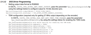
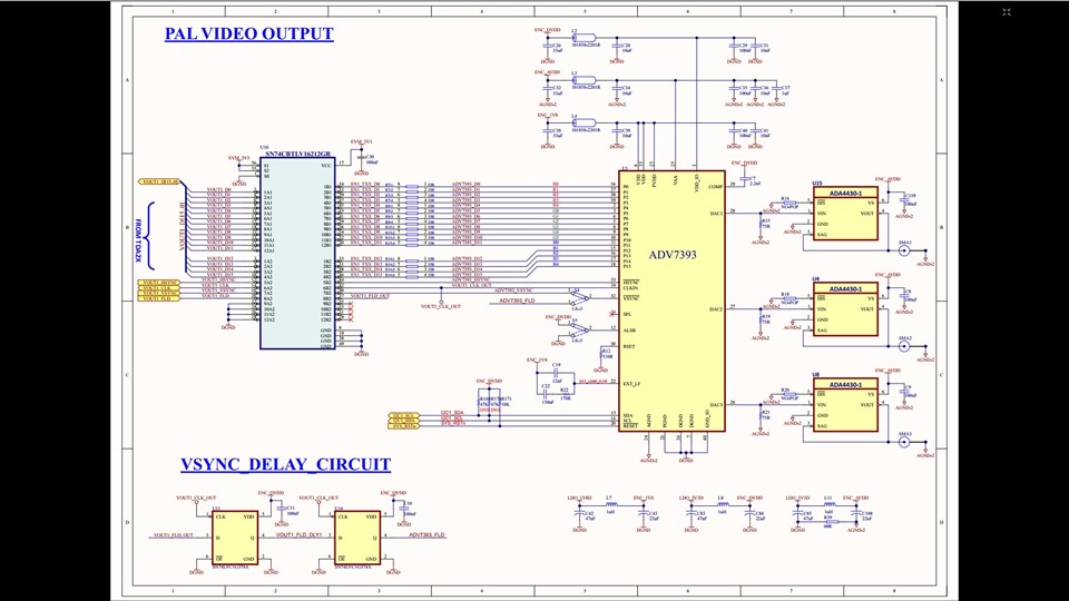
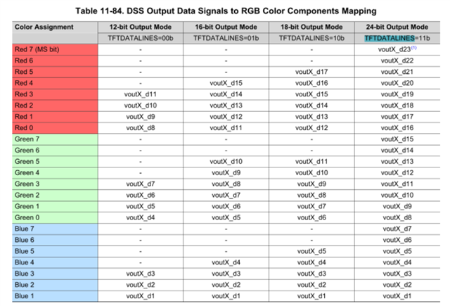
I want to use ADV7393 to get PAL output at my video output port from TDA2x DSS. I have made the schematics. I just want to get a review of this schematic. I have connected D0 to D15 to P0 to P15 of the encoder. The reset I am using is generated by a programmable delay IC. HS is directly from VOUT1 to HS of ADV. As far as VS is concerned, I have added the D-FLIP FLOPs (to delay FLD) as suggested by appnote and connected the output to VS of ADV. Kindly review my schematics (I have attached) and suggest any change (if any) so that I could finalize my design.



 See attachment: