This thread has been locked.

If you have a related question, please click the "Ask a related question" button in the top right corner. The newly created question will be automatically linked to this question.

[FAQ] AM625 / AM623 / AM62A / AM62P Design Recommendations / Commonly Observed Errors during Custom board hardware design – SOC Unused peripherals and IOs

Part Number: AM625

Hi TI Experts,

I am designing my custom board using TI AM62x family of processors. I have a few queries.

1. I am expecting to not use some of the SOC peripherals. Do you have a recommendation?

2. We have a general recommendation to add a pull down to unused AM64x I/O that has test points on it. This is a bit unexpected for me to see as well. How critical is this. What if customer instead enables the internal weak pull-down, or configures the I/O as an output? Does that remove the need for an external pull-down.

3. Our assumption for the recommendations is that we are just wanting to prevent noise coupling onto the unterminated trace.

4. Is there any concern connecting a capacitor or connecting an external slow ramp input to the SOC IOs or Reset inputs.

5. Is it allowed to connect a capacitor at the output of the SOC IO

6, Recommend pull value for SOC IOs that drives an attached device inputs that could float 

  • Hi Board designers, 

    Refer below inputs:

    1. I am expecting to not use some of the SOC peripherals. Do you have a recommendation?

    Refer to the Pin Connectivity Requirements of the device specific data sheet.

    Common SOC LVCMOS IO interface guidelines

    1. Most of the SOC IOs are not fail-safe. No input should be applied before supply ramps.
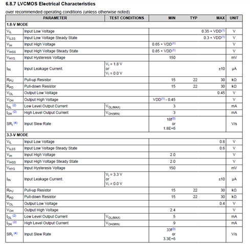
    2. SOC LVCMOS inputs have minimum slew rate requirements specified
    3. SOC IO buffers are off during Reset. A pull is required near to the attached device being
    driven by the SOC IOs
    4. Any SOC IO that has a trace connected and not being actively driven needs a parallel pull.

    2. We have a general recommendation to add a pull down to unused AM64x I/O that has test points on it. This is a bit unexpected for me to see as well. How critical is this. What if customer instead enables the internal weak pull-down, or configures the I/O as an output? Does that remove the need for an external pull-down.

    It is OK to leave any of the SOC IO that are not used unconnected. When no trace is connected to the SOC pads, no external pulls are required or recommended. We are recommending an external pull for any SOC IO that has a trace connected but not being actively driven.

    2.1 Is there an alternative suggestion when adding pulls is not feasible 

    When adding pull is not feasible, ensure the traces are routed away from noisy signals

    3. Our assumption for the recommendations is that we are just wanting to prevent noise coupling onto the unterminated trace.

    This is correct. This may have design dependencies including the board design. The recommendation also come due to the process node used in AM62x.

    Additional Explanation

    The SoC IO buffers are off (high impedance) during power up. The pulls have to configured after boot by the software.
    It is not a good design practice to leave unterminated signal traces connected to the SOC pins. Without any termination, these signals are very high impedance. This makes it easy for noise to couple energy on these floating signal trace and develop a potential that could exceed our recommended operating conditions, which would create an Electrical Over-Stress (EOS) on the IOs.
    This signal in the example system described below is effectively an antenna that will pick up noise. A potential will be generated on the signal when noise couples into the antenna. This potential will be largest on the highest impedance end of the signal. By placing a pull-up or pull-down near the SoC, we force the highest potential to the open-circuit end of the signal rather than the SoC end of the signal.

    It is easy to induce a voltage potential on floating signals because the impedance is very high when not pulled or driven to a valid logic level. A potential can be induced by simply exposing the floating signal trace to an electric field. For example, if you have an unterminated conductor located between two other conductors that have a potential difference the electric field between these conductors will terminate on the unterminated conductor and cause the unterminated conductor to rise to a potential that is proportional to the distance between the two conductors with a potential difference. This is the reason we must always protect PCB assemblies with semiconductors installed, by placing the assembly in a conductive/static dissipative bag. Circuits on the PCB may experience an Electrical Over-Stress (EOS) without anyone or anything actually touching the PCB, by simply exposing the PCB assembly to a strong electric field. Normally you would only remove the PCB assembly from the conductive/static dissipative bag as it is being install it in the product enclosure at an ESD workstation, where the PCB should be protected once inserted in its product enclosure. The expectation is that the product designer controls the electric fields within the product enclosure such that no circuits are exposed to an EOS event. Therefore, it may be possible to leave signals floating if the product designer can ensure these floating signals are never exposed to an electric field that is strong enough to induce a potential capable of creating an EOS event. This is basically a system level design decision that needs to be considered by the product designer. However, installing pull resistors on these signals will significantly reduce the chance of them rising to a potential that creates and EOS event.

    4. Is there any concern connecting a capacitor or connecting an external slow ramp input to the SOC IOs or Reset inputs.

    SOC IOs have slew rate requirements as shown below. IT is recommended to follow the below recommendation and perform simulations or measurements to understand the allowed cap value.

    When slow ramp input is applied, CMOS input will have shoot-through current that flows from VDD through the partially turned-on P-channel transistor and the partially turned-on N-channel transistor to VSS when the input is at mid-supply. Accumulated exposure to slow ramps could result in performance or reliability concerns.

    5. Is it allowed to connect a capacitor at the output of the SOC IO

    LVCMOS output buffers were not designed to drive large capacitive loads. For LVCMOS type IOs when configured as output and connected to capacitive load, follow the data sheet recommendations for the allowed capacitor value or add series resistor to limit the current or perform simulations.

    6, Recommend pull value for SOC IOs that drives an attached device inputs that could float 

     On a bidirectional signal it doesn’t matter where the pulls are located on the signal traces as long as they are connected such that they do not introduce stubs on the signal. If the signal is unidirectional, it is recommended to have the pulls located closer to the receiver.

    47K pulls should be okay, pull value is use case dependent. Customer should verify if their product will be exposed to high strength energy fields that are able to couple enough noise into their PCB signal traces and over-drive the 47k pulls. A 10K is recommended in these use case.

    Regards,

    Sreenivasa

  • Hi Board designers, 

    Here are some guidelines that needs to be considered when selecting or designing the SOC power architecture

    • Power supplies are configured to the required voltage level and are supplies are within the ROC
    • Power architecture follows the power-up and power-down sequence as specified in the SOC data sheet
    • Power architecture meets the slew rate requirements as specified in the SOC data sheet
    • Ensure all the power supplies are available before the MCU_PORz is released
    • Monitoring of all the supply rails
    • Ensure the supplies are turned ON only after the voltage is below 0.3V (no residual voltage) after a power cycle
    • The delay between the power supply ramp and the MCU_PORz high is as per the data sheet recommendations (9.5 ms min)
    • The MCU_PORz slew is as minimum as possible to avoid internal reset circuit glitch

    Regards,

    Sreenivasa