This thread has been locked.

If you have a related question, please click the "Ask a related question" button in the top right corner. The newly created question will be automatically linked to this question.

AM625: AM625 transient overshoot and undershoot at IO pins

Part Number: AM625

I have a question about the maximum value of overshoot and undershoot on IO pins.


In the datasheet of the component is defined a value of "steady-state max voltage" that must be between -0.3V and "IO supply voltage "+0.3V.


A value for "transient overshoot and undershoot at IO pin" is given below. This value is 0.2xVDD. The maximum time should be 20% of the signal period.


On the other hand, the value of VDDSHVx must be between +1.71V and +1.89V.


Now, if VDDSHVx is +1.71V, the transient undershoot cannot be less than -0.342V for 20% of the signal period. However, it can remain indefinitely at -0.300V indefinitely. Is this correct?


Does the maximum undershoot value depend on the supply voltage itself?


For other devices (e.g. FPGA) the manufacturer usually provides a table that relates the undershoot voltage to the percentage of the signal period. Does Texas Instruments provide such a table?


Regards

  • Hello Amílcar Barca

    Thank you for the query.

    Now, if VDDSHVx is +1.71V, the transient undershoot cannot be less than -0.342V for 20% of the signal period. However, it can remain indefinitely at -0.300V indefinitely. Is this correct?

    This is correct.

    Does the maximum undershoot value depend on the supply voltage itself?

    (7) VDD is the voltage on the corresponding power-supply pin(s) for the IO.

    For other devices (e.g. FPGA) the manufacturer usually provides a table that relates the undershoot voltage to the percentage of the signal period. Does Texas Instruments provide such a table?

    Could you please share or point to the table that you mentioned for me to check on the availability with the device experts.

    Regards,

    Sreenivasa

  • Hi,

    It seems a bit strange that the maximum undershoot level (with respect to GND) depends on the voltage on the VDDSHVx supply pin.

    It seems a bit strange that the maximum undershoot level (with respect to GND) depends on the voltage on the VDDSHVx supply pin.On the other hand, going into conduction the internal ESD protection diodes, I understand that more than the voltage, a V-t area should be given. After all, the stress on the diodes is due to the energy they must dissipate when they go into conduction.

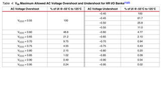
    For a XILINX Artix-7 FPGA, they are giving such a table:

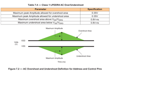
    For other ICs, such as an LPDDR4 memory, an area is specified: it looks much more correct to me.

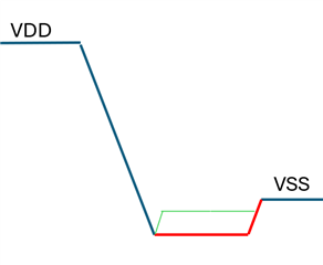
    If you just define a peak voltage value and an undershoot time, you come to the conclusion that the stress level is the same in either of the two conditions I attached (green and red).

    But I don't think it is the same.

    Regards.

  • Hello Amílcar Barca

    Thank you for the inputs.

    Let me review the inputs and also reach out to the device expert to get his thoughts.

    Regards,

    Sreenivasa

  • I discussed your questions with our IO designer.

    I was told the answer to your first question is yes. The signal can be -0.3 indefinitely.  Apparently, the absolute max limits mirror JEDEC standard values which allow ground/supply potential differences among the transmitter (external device) and receiver (TI device).

    The overshoot value is calculated based on the following formula. [Recommended Operating Conditions (ROC) MAX value + (0.2 x ROC NOM value)]. For example, the peak overshoot for an input operating at 1.8V will be [1.89V + (0.2 x 1.8V)] = 2.25V. The peak undershoot will have negative symmetry relative to 0V. The peak undershoot will be -0.45V if you apply the peak overshoot value of (2.25V - 1.8V) = 0.45V as an undershoot relative to 0V.

    I was told we do not have a table that defines overshoot/undershoot limits based on duration. We only define the limit defined in the datasheet.

    Regards,
    Paul