Other Parts Discussed in Thread: SYSCONFIG
Hello,
I was wondering what the default clock source is for the WKUP_GTC0 interface? The EVM appears to route this out to an expansion header by default and I just want to make sure I am following the signal/source names correctly through the TRM.
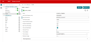
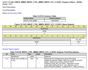
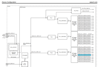
- The WKUP_CTRL_MMR0_WKUP_GTC_CLKSEL register is stating that MAIN_PLL2_HSDIV5_CLKOUT is most likely the default option if the register bits [2-0] = 000.
- Chasing MAIN_PLL2_HSDIV5_CLKOUT down seems to indicate that it is generated by MAIN_PLL2_REF_CLK.
- MAIN_PLL2_REF_CLK looks like it comes from MCU_HFOSC0 which is part of the MCU domain.
- MCU_HFOSC0 is generated by the source connected to the MCU_OSC0_XI pin.
Figure 6-92 for reference
Questions
- So on the EVM this appears to be the 25MHz crystal (Y1)?
- Are there any extra clock dividers happening by the time is gets to the WKUP_GTC0 interface?
Thank You,
Spencer