This thread has been locked.

If you have a related question, please click the "Ask a related question" button in the top right corner. The newly created question will be automatically linked to this question.

TDA4VL-Q1: Trace_analysis

Part Number: TDA4VL-Q1
Other Parts Discussed in Thread: TDA4VL

Hello , 

we need to configure the TRACE_CLK 

1-The Register PADCONFIG_1 with address 0x4301C004 , I configured it as Output with value 10 to enable the CLK

2-The Register PADCONFIG_50 with 0x4301C0C8 , I configured it as Output with value 10 to enable the CLK
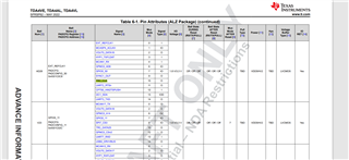
This is the right configuration or we need something else?

Also I need to know the names of  ETM register need to be configured through the Isystem Debugger?

  • Hello,

    I was asked to review this but was out of the office last week.

    I've attached the JTAG script I use with TRACE32 to configure the TRC pins for ETM (and system trace) on TDA4VL on the TI-EVM.  You will need to know use your boards schematic to know which pins to setup, you will also need to know the width your trace receiver can accept.  The TDA4L exports up to 26 bits of data trace but the EVM only exports 21 bits.  For M core debug usually 1-4 bits is OK, where a R core might want 8-16.  The A cores or concurrent trace may use all of the pins you can provide.

    https://e2e.ti.com/cfs-file/__key/communityserver-discussions-components-files/791/J721S2_5F00_offchip_5F00_trace.cmm

    As to what is proper for the iSystems debugger, you should talk with their (iSystems/Tasking) support.

    Regards,
    Richard W.

  • Hello Richard ,

    Thanks for your support, 

    I want to know how we can use this script , if we need to put it in a specific path while we downloading or flashing the software? or how we can use this JTAG script?

  • Hello Emad,

    The example JTAG script that I attached is for use with Lauterbach's TRACE32.  It is run after an attach has happened to any of the cores on the TDA4VL (Cortex-M4, DSP-C7x, Cortex-R5, Cortex-A72).  The script sets up some tool settings, then does the pin mux, then kicks off a receiver training.  You mentioned you were using an iSystems debug box.  This script will not directly work with that and some porting of the logic would need to happen for that tools environment. I know that iSystems boxes support TDA4 through work with them and other customers so you should be able to ask iSystems/Tasking for support on this.  I do not have one of those systems to offer any detailed feedback into their tools APIs and syntax.

    Regards,
    Richard W.
  • Hello Richard,

    I configured the Pins of the CLK as the following screenshot, but when I measured the PIN W25 on the SOC , I found that the PIN is HIGH all the time, there is no change , is there is an extra configuration I need to add it , to see the CLK pulses?

  • please see the channel D7

  • Hello Emad,

    On the TI-EVM there is a FET-MUX used to select between trace and alternate functions.  That MUX's initial state is set by a board DIP switch, but that value can be overridden by an I2C-GPIO-expander signal.  If you are testing on an EVM, you need to ensure the MUX select signal is correct.  If you are trying on your own board, and the connectivity matches the EVM, then you will need to also ensure the trace clock is active before you might see any transitions on the TRC_CLK line.  In general, the TPIU has a pattern generator which a debug box will activate to generate a test pattern to train against.  The checkout should be to setup the clocks, then setup any MUX routing (board level and SOC level), then use the tool to generate a test pattern.  You can probe the header to see the clock then, or you can use some tool level information to deduce if things are toggling.

    Regards,
    Richard W.

  • Hello Richard ,

    Could you please inform me about the the alternative PINs of the EVM in the SOC to be able to configure them because I am working on my own board .

  • Hello Emad,

    I am not following your question as written.  The EVM is provisioned so the TRC pins route to potential daughter boards.  The EVM chose to add special high speed FET-MUXes to provide signal routes to each function. These MUXes are controlled by a A/B/C selector (dip switch or gpio controllable).  Some EVMs do the same but add/remove resistors to get the same effect.   If your own board can dedicate signals that is the more simple and you only need to ensure the SOC level pad functions are setup properly (along with proper clocks to internal units).

    Regards,
    Richard W.