This thread has been locked.

If you have a related question, please click the "Ask a related question" button in the top right corner. The newly created question will be automatically linked to this question.

PROCESSOR-SDK-AM64X: GPIO Configuration

Part Number: PROCESSOR-SDK-AM64X
Other Parts Discussed in Thread: AM2434

Hello,

I have a question regarding GPIO configurations on the AM64x/AM64243x.

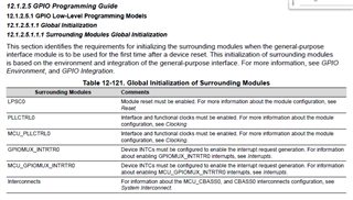
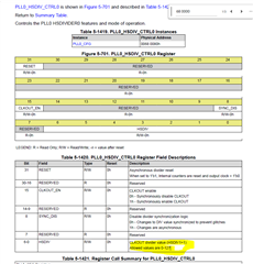
In the GPIO Programming Guide section of the reference manual (section 12.1.2.5), there is a Global Initialization sub section (12.1.2.5.1.1). The Table 12-121 describes the need to initialize tje surrounding modules before initializing any of the GPIOs. It talks about enabling the module reset and enabling the interface and functional clocks.

Can you please explain how and what registers need to be written to in order to configure those? I can't seem to find anything in the API that explains how to do this.

I inserted a picture of the table in question.

Thank you!

  • Hello,

    Which SDK are you using, Linux or MCU+? This will help us assign to the correct person to respond.

    Thanks,

    Anshu

  • Thanks. This thread will be re-assigned to the correct expert. Please allow some time for a response.

    Best Regards,

    Anshu

  • Hello Eden Abitbol,

    I am sure that you no need to control above registers since there is SSYFW is avialble on AM64X and which does all opeations setting PLL Clocks , setting operating frequency for diferent cores and periperhals ,resoucer allocations ,  reset and other security features will handle by the SYSFW and it run on M3 core .

    So, to use GPIO's you no need to controlany above registers and simply configure GPIO in input or ooupur or interrupt in Application or SBL from system cfg and it wil generated code to configure GPIO peripehrals registers other than this you no need to do anything .

    Please let me know if this helps your query .

    You can look at the image below all PLL setting has configured to all GPIO's in the SYSFW and you don't need to enable them again .

    So, to use GPIO's you don't need to control any above registers and simply configure the GPIO as input or output or interrupt in Application or SBL from system cfg, and it will generate code to configure GPIO peripherals registers other than this you no need to do anything.

    Please let me know if this helps your query.

    You can look at the image below all PLL setting has configured to all GPIO's in the SYSFW and you don't need to enable them again .

    https://dev.ti.com/sysconfig/#/config/?args=--product%20%2Fmnt%2Ftirex-content%2Fsitara_ctt_1_1_1%2F.metadata%2Fproduct.json%20--device%20AM64x%20--part%20Default%20--package%20ALV%20--context%20system

    Regards,

    Anil.

  • Ok so let's assume that the system cfg set's all the PLLs correctly, I have another question concerning the GPIO interrupts. In the datasheet for the am2434, there is a table that illustrates the pulse width requirements for generating gpio interrupts. In my case, I'm configuring a GPIO as an input that will receive  a signal from another board. That signal will be used to trigger an interrupt with on a falling edge. The table below (from the datasheet) specifies, for 3.3V, that the minimum pulse width required is 2P +3.5 where P is the functional clock in ns.

    How and where do I set this functional clock?

  • Hello Eden,

    Please look at the below image and clock tree link.

    The 125MHz clock is connected to GPIO modules as per the clock tree.

    So, your functional clock is 125MHz.

    Please don't change this PLL clock. If you change this PLL clock, then this will affect all peripherals.

    Regards,

    Anil.

  • I looked at the clock tree. MCU_SYSCLKOUT0 is set to 25 mhz which will set the clock for the GPIO to 125 mhz after the PLLs. However, I am using the GPIOs from the MAIN module. So instances GPIO0 and GPIO1, not MCU_GPIO.

    From the following figure and table


    you can see that the GPIO0_VBUS_CLK and GPIO1_VBUS_CLK come from the MAIN_SYSCLK0 whichc comes out of PLLCTRL0.

    You can also look at this block diagram

    which illustrates this. From the table of the GPIO configurations above, you can see the clock comes from PLLCTRL0, not from the HSDIVs. This is why I'm asking for clarifications as to which clock and frequency is servicing the MAIN_GPIO0 and MAIN_GPIO1.

    If we are using a 25 mhz crystal (MCU_HF0SCO_CLKOUT), what are the corresponding PLLs and what is the MAIN_SYSCLK0 for the MAIN GPIO modules?

  • Hello Eden,

    Thanks for sharing the above details.

    After seeing the above images and clock tree I also got confused about which clock we are feeding to GPIO Modules.

    As per TRM, we feed MAIN_SYS_CLK to the GPIO Module, but in the clock the tree we are feeding the HSDIV0 clock to GPIO.

    So, we can just follow the TRM. As per TRM, the MAIN SYS CLOKC is going to GPIO and other peripheral modules.

    Now, MAIN SYS CLOKC frequency is equal to 125MHz. The same frequency is divided by 4 times as it going to the GPIO modules.

    clock tree is not connected to the sysclock out to GPIO and other periperhals, and it is connected to 500MHz clock 

    I assume that clock tree seems wrong. I will confirm one more time and let you know.

    Unfortunately, this MAIN SYS CLK is internal to SOC and to capture frequency on this pin is not possible.


    Regards,

    Anil.

  • How can the MAIN_SYSCLK be 125 mhz if the crystal is generating 25 mhz into the MCU_HFOSC0_CLKOUT?

  • Hello Eden,

    Please look at the image below.

    For the MCU_PLLCONTRL0 there are two inputs are coming one from 25MHz and another one from HSDIV0 which is 500MHz.

    The same should come for PLLCTRL0, but there seems like mistakes in TRM.

    I checked on the clock tree for PLLCTRL0 inputs where it was mentioned properly.

    So, 25MHz and 500MHZ clocks are feeding to PLLCTRL0 as well from these 3 outputs are coming.

    And, you can look at the system's_clock_out value.

    Based on this information I am telling you this value is 125MHz.

    Regards,

    Anil.