TDA4VH-Q1: Bus error

Part Number: TDA4VH-Q1
Other Parts Discussed in Thread: TDA4VM

Tool/software:

Hi Ti,

Regarding the issue of a Bus error occurring after mapping PCIe BAR to process space and accessing it, there has been new progress.

Using gdb debugging, it was found that every time the assembly instruction “str q0, [x1]” is executed, a Bus error occurs, where x1 = 0xfffff7f90028. The address after the process mmap PCIe BAR is 0xfffff7f90000. This address appears to be eight-byte aligned. I am not sure why this assembly instruction causes a Bus error. Moreover, I have checked that the address range 0xfffff7f90000-0xfffff7fA0000 has rw-s permissions before executing this instruction.

What is even more puzzling is that when running with valgrind, no Bus error occurs, and the execution completes normally without any errors in the result check. I wonder if this issue is related to PCIe. Could experts from TI help analyze this?

Regards,

Qiang

  • Hi Qiang,

    Thank you for trying out some experiments and looking into this issue on your end. If running with Valgrind does not cause issues, it may be related to timing.

    One experiment we could try is to build the PCIe driver as a module and load it in at runtime instead of boot.

    Regards,

    Takuma

  • Hi Takuma,

    Although I don't understand why this issue is related to timing, I tried your suggestion. One experiment we could try is to build the PCIe driver as a module and load it at runtime instead of at boot. This experiment has the same effect as compiling the PCIe driver into the kernel. I really need your help; this issue has been troubling me for a long time. This issue occurs when using C++'s placement new operator to create an object at the address returned by mmap, and it happens before the constructor is executed. This means the error might occur while allocating memory for the class members. I have simplified the class members and found several instances where a Bus error is triggered. These errors seem to follow a pattern with instructions like 'str q0, [x1]', where q0 is stored at an address ending in 0x******8.

    Regards,

    Qiang

  • Hi Qiang, 

    Thanks for trying out the experiment. Had suspicion on timing since you mentioned running with Valgrind did not cause any issues, so thought there might be some other software dependencies that are getting loaded.

    As for the new information, may be something to do with alignment and/or we are mapping some region that should not be accessed in device tree somehow.

    Regards,

    Takuma

  • Hi Takuma,

    Thank you for your reply. Today I investigated the device tree and alignment issues. I checked the device tree configuration and found no problems. I then tried aligning all classes with class alignas(*) xxx, using * = 8 resulted in a bus error, but using * = 16 did not cause a bus error, although it caused a hang. I suspect the issue might be with the mutex not functioning properly. Therefore, I would like to confirm a few questions:

    1. Why is 16-byte alignment required?
    2. Is this alignment requirement determined by the driver? If so, please let me know where it is configured.
    3. When users access PCI BAR space using mmap, do they need a specific alignment? Can't it be accessed as freely as DDR?
    4. If a mutex is placed in mmap PCI BAR space, can it function properly?


    Regards,

    Qiang

  • Hi Qiang,

    There is a section in the TRM named "12.2.3.3.6.2 PCIe Transaction Limitations". I see some limitations in terms of alignments such as:

    • Transaction Address Alignment
    The PCIe subsystem imposes a limitation of a maximum of 128-byte outbound read/write command. However,
    if the starting address is not aligned to an 8-byte boundary, then the maximum transaction size is reduced to
    120 bytes. This limitation is placed to avoid arithmetic overflow in computing transaction length from CBA to AXI.
    Unspecified behavior will occur, if misaligned transactions in outbound direction are not limited to a maximum of
    120 bytes.

    • Byte Strobe Limitations
    For any type of write transactions, the byte enables can only have a single unbroken string of 1s. In other words,
    in a transaction, if a byte’s write strobe is set, then all following bytes must have write strobe set until the last
    byte with write enabled. "Holes" or "Zeros" in between the byte enables are not allowed.
    Since the internal bus width is greater that 32-bit, the TLP (Transaction Layer Packets) size will not be 1 (PCIe
    counts in 32-bit units) and therefore, it is through the FBE/LBE (First/Last Byte Enable) that the actual data
    transfer size is controlled.

    It may be that we are hitting one of these.

    Regards,

    Takuma

  • Hi Takuma,

    Thank you very mush for your assistance.Through debugging, I've found that memcpy and memset often result in bus errors, especially on odd byte boundaries. However, performing individual assignment operations doesn't lead to bus errors. I can't understand why this is happening. Could it be related to the byte enable you mentioned? Isn't byte enable meant to address memory fragmentation issues?

    Regards,

    Qiang

  • Hi Qiang,

    It might be, but do you happen to have a PCIe protocol analyzer at your company? Inspecting the TLP packets should let us know what FBE/LBE is being set.

    Regards,

    Takuma

  • Hi Takuma,
    Our company does not have a PCIe protocol analyzer. Are there specific rules that must be followed when using mmap for PCIe space? Is it not as flexible as using regular memory? This seems to be a common issue, right? How do others handle this? I would like to know how to make it as easy for users to use it as regular memory, without needing to understand PCIe rules before writing code.

    Regards,

    Qiang

  • Hi Qiang,

    Our company does not have a PCIe protocol analyzer.

    Understood.

    How do others handle this?

    I will have to look a little more deeply into drivers, but our EP/RC driver uses this:

    https://github.com/torvalds/linux/blob/master/drivers/pci/endpoint/functions/pci-epf-test.c#L806

    Regards,

    Takuma

  • Hi Takuma,

    The driver at https://github.com/torvalds/linux/blob/master/drivers/pci/endpoint/functions/pci-epf-test.c#L806 does not meet my usage requirements. We expect users to be able to use PCIe space as if it were regular memory, so we implemented the mmap interface in the driver.

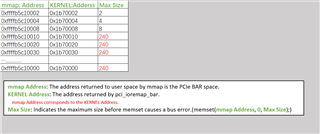
    I wrote a very simple test program in the application layer. First, I open the PCIe device, then mmap the starting space of the PCIe BAR. Finally, I use the address returned by mmap, apply an offset, and pass it to memset for zeroing. I found that regardless of how the address is aligned, the maximum size passed to memset is only 240 bytes. When the address alignment is less than 16 bytes, the maximum size passed to memset is reduced to less than 8 bytes. I don't know why this is happening. I have listed a table for reference.


    Regards,

    Qiang

  • Hi Qiang,

    The data you have shared is quite interesting in the fact that 240 is a multiple of 120. As I mentioned before, based on the TRM, 120 is the max transaction size that is allowed if not aligned to an 8-byte boundary. Additionally, 128 (or in the case of mis-aligned 120) bytes is the max payload size, meaning 240 is precisely the max size for 2 mis-aligned packets instead of 1. 

    This may or may not be related to the issue... could you dump PCIE_RC_i_rc_pcie_base_i_pcie_dev_ctrl_status register content? This should have maximum TLP payload size that is configured. Register address is 0xD0000C8, 0x0D8000C8, 0x0E0000C8, 0x0E8000C8 for PCIe0, 1, 2, 3 respectively.

    Regards,

    Takuma

  • Hi Takuma,

    All 240 bytes are aligned to 8-byte addresses. I suspect another situation: the 240 bytes are the payload, and with the TLP Header and Digest/ECRC, it adds up to 256 bytes. Coincidentally, the DevCap: MaxPayload is also 256 bytes. However, MaxPayload refers to the effective payload and does not limit the TLP size.

    Regarding the MP register you mentioned, I checked its value, and it is 0, which should correspond to 128 bytes. Changing it to 1 did not help with my problem.

    There are no AER errors when the bus error occurs.

    Using memset_io/memcpy_toio in the driver does not cause errors, regardless of the size, but these require specific I/O interfaces. I am unsure what happens after using memset in user space because it does not use the specific I/O interfaces.

    Regards,

    Qiang

  • Hi Quant,

    To clarify, these are memory write requests that are being sent and not IO, device, or config requests correct?

    And the error only happens at 64-bit memory addresses?

    Regards,

    Takuma

  • Hi Takuma,

    Yes. The address being operated on is a 64-bit address returned by mmap of the PCIe BAR in user space. From the user's perspective, performing memset is a write operation to memory. However, this address is mapped to the PCIe BAR space of the endpoint (EP). I understand that such a write operation at the lower level should access the PCIe BUS and thus operate the device. I am not very clear about the specific details of how this is done at the lower level.

    Regards,

    Qiang

  • Hi Qiang,

    Thanks for the clarification. I just found a set of registers that may be interesting to look at. Could you dump the following registers:

    0D10 0300h 0D90 0300h 0E10 0300h 0E90 0300h 32 100300h CORE_DBN_CFG_PCIE_CORE PCIE_LM_i_regf_lm_pcie_base_i_rc_BAR_config_reg
    0D10 0300h 0D90 0300h 0E10 0300h 0E90 0300h 32 100300h CORE_DBN_CFG_PCIE_CORE PCIE_LM_i_regf_lm_pcie_base_i_rc_BAR_config_reg
    0D10 0300h 0D90 0300h 0E10 0300h 0E90 0300h 32 100300h CORE_DBN_CFG_PCIE_CORE PCIE_LM_i_regf_lm_pcie_base_i_rc_BAR_config_reg
    0D10 0300h 0D90 0300h 0E10 0300h 0E90 0300h 32 100300h CORE_DBN_CFG_PCIE_CORE PCIE_LM_i_regf_lm_pcie_base_i_rc_BAR_config_reg
    0D10 0300h 0D90 0300h 0E10 0300h 0E90 0300h 32 100300h CORE_DBN_CFG_PCIE_CORE PCIE_LM_i_regf_lm_pcie_base_i_rc_BAR_config_reg
    0D10 0300h 0D90 0300h 0E10 0300h 0E90 0300h 32 100300h CORE_DBN_CFG_PCIE_CORE PCIE_LM_i_regf_lm_pcie_base_i_rc_BAR_config_reg
    0D10 0300h 0D90 0300h 0E10 0300h 0E90 0300h 32 100300h CORE_DBN_CFG_PCIE_CORE PCIE_LM_i_regf_lm_pcie_base_i_rc_BAR_config_reg
    0D10 0300h 0D90 0300h 0E10 0300h 0E90 0300h 32 100300h CORE_DBN_CFG_PCIE_CORE PCIE_LM_i_regf_lm_pcie_base_i_rc_BAR_config_reg
    0D10 0300h 0D90 0300h 0E10 0300h 0E90 0300h 32 100300h CORE_DBN_CFG_PCIE_CORE PCIE_LM_i_regf_lm_pcie_base_i_rc_BAR_config_reg
    0D10 0300h 0D90 0300h 0E10 0300h 0E90 0300h 32 100300h CORE_DBN_CFG_PCIE_CORE PCIE_LM_i_regf_lm_pcie_base_i_rc_BAR_config_reg
    0D10 0300h 0D90 0300h 0E10 0300h 0E90 0300h 32 100300h CORE_DBN_CFG_PCIE_CORE PCIE_LM_i_regf_lm_pcie_base_i_rc_BAR_config_reg

    Regards,

    Takuma

  • Hi Takuma,

    I am using PCIe 1. The register address of PCIE_LM_i_regf_lm_pcie_base_i_rc_BAR_config_reg is 0x0D900300. The corresponding register value is 0x001E0000.

    Regards,

    Qiang

  • Hi Takuma,

    Supplement RC's lspci information

    0000:00:00.0 PCI bridge: Texas Instruments Device b00d (prog-if 00 [Normal decode])
            Control: I/O- Mem+ BusMaster+ SpecCycle- MemWINV- VGASnoop- ParErr- Stepping- SERR- FastB2B- DisINTx+
            Status: Cap+ 66MHz- UDF- FastB2B- ParErr- DEVSEL=fast >TAbort- <TAbort- <MAbort- >SERR- <PERR- INTx-
            Latency: 0
            Interrupt: pin A routed to IRQ 36
            Bus: primary=00, secondary=01, subordinate=01, sec-latency=0
            I/O behind bridge: [disabled]
            Memory behind bridge: 18100000-1fdfffff [size=125M]
            Prefetchable memory behind bridge: [disabled]
            Secondary status: 66MHz- FastB2B- ParErr- DEVSEL=fast >TAbort- <TAbort- <MAbort- <SERR- <PERR-
            BridgeCtl: Parity- SERR+ NoISA- VGA- VGA16- MAbort- >Reset- FastB2B-
                    PriDiscTmr- SecDiscTmr- DiscTmrStat- DiscTmrSERREn-
            Capabilities: [80] Power Management version 3
                    Flags: PMEClk- DSI- D1+ D2- AuxCurrent=0mA PME(D0+,D1+,D2-,D3hot+,D3cold-)
                    Status: D0 NoSoftRst+ PME-Enable- DSel=0 DScale=0 PME-
            Capabilities: [90] MSI: Enable+ Count=1/1 Maskable+ 64bit+
                    Address: 0000000001040000  Data: 0000
                    Masking: 00000000  Pending: 00000000
            Capabilities: [b0] MSI-X: Enable- Count=1 Masked-
                    Vector table: BAR=0 offset=00000000
                    PBA: BAR=0 offset=00000008
            Capabilities: [c0] Express (v2) Root Port (Slot+), MSI 00
                    DevCap: MaxPayload 256 bytes, PhantFunc 0
                            ExtTag- RBE+
                    DevCtl: CorrErr+ NonFatalErr+ FatalErr+ UnsupReq+
                            RlxdOrd+ ExtTag- PhantFunc- AuxPwr- NoSnoop+
                            MaxPayload 256 bytes, MaxReadReq 512 bytes
                    DevSta: CorrErr- NonFatalErr- FatalErr- UnsupReq- AuxPwr- TransPend-
                    LnkCap: Port #0, Speed 8GT/s, Width x2, ASPM L1, Exit Latency L1 <8us
                            ClockPM- Surprise- LLActRep- BwNot+ ASPMOptComp+
                    LnkCtl: ASPM Disabled; RCB 64 bytes Disabled- CommClk-
                            ExtSynch- ClockPM- AutWidDis- BWInt- AutBWInt-
                    LnkSta: Speed 8GT/s (ok), Width x2 (ok)
                            TrErr- Train- SlotClk- DLActive- BWMgmt+ ABWMgmt-
                    SltCap: AttnBtn- PwrCtrl- MRL- AttnInd- PwrInd- HotPlug- Surprise-
                            Slot #0, PowerLimit 0.000W; Interlock- NoCompl-
                    SltCtl: Enable: AttnBtn- PwrFlt- MRL- PresDet- CmdCplt- HPIrq- LinkChg-
                            Control: AttnInd Off, PwrInd Off, Power+ Interlock-
                    SltSta: Status: AttnBtn- PowerFlt- MRL+ CmdCplt- PresDet- Interlock-
                            Changed: MRL- PresDet- LinkState-
                    RootCap: CRSVisible-
                    RootCtl: ErrCorrectable- ErrNon-Fatal- ErrFatal- PMEIntEna+ CRSVisible-
                    RootSta: PME ReqID 0000, PMEStatus- PMEPending-
                    DevCap2: Completion Timeout: Range B, TimeoutDis+, NROPrPrP-, LTR+
                             10BitTagComp+, 10BitTagReq-, OBFF Not Supported, ExtFmt+, EETLPPrefix+, MaxEETLPPrefixes 1
                             EmergencyPowerReduction Not Supported, EmergencyPowerReductionInit-
                             FRS-, LN System CLS Not Supported, TPHComp-, ExtTPHComp-, ARIFwd+
                             AtomicOpsCap: Routing- 32bit- 64bit- 128bitCAS-
                    DevCtl2: Completion Timeout: 50us to 50ms, TimeoutDis-, LTR+, OBFF Disabled ARIFwd+
                             AtomicOpsCtl: ReqEn- EgressBlck-
                    LnkCtl2: Target Link Speed: 8GT/s, EnterCompliance- SpeedDis-
                             Transmit Margin: Normal Operating Range, EnterModifiedCompliance- ComplianceSOS-
                             Compliance De-emphasis: -6dB
                    LnkSta2: Current De-emphasis Level: -6dB, EqualizationComplete+, EqualizationPhase1+
                             EqualizationPhase2+, EqualizationPhase3+, LinkEqualizationRequest-
            Capabilities: [100 v2] Advanced Error Reporting
                    UESta:  DLP- SDES- TLP- FCP- CmpltTO- CmpltAbrt- UnxCmplt- RxOF- MalfTLP- ECRC- UnsupReq- ACSViol-
                    UEMsk:  DLP- SDES- TLP- FCP- CmpltTO- CmpltAbrt- UnxCmplt- RxOF- MalfTLP- ECRC- UnsupReq- ACSViol-
                    UESvrt: DLP+ SDES+ TLP- FCP+ CmpltTO- CmpltAbrt- UnxCmplt- RxOF+ MalfTLP+ ECRC- UnsupReq- ACSViol-
                    CESta:  RxErr- BadTLP- BadDLLP- Rollover- Timeout- AdvNonFatalErr-
                    CEMsk:  RxErr- BadTLP- BadDLLP- Rollover- Timeout- AdvNonFatalErr+
                    AERCap: First Error Pointer: 00, ECRCGenCap+ ECRCGenEn- ECRCChkCap+ ECRCChkEn-
                            MultHdrRecCap- MultHdrRecEn- TLPPfxPres- HdrLogCap-
                    HeaderLog: 00000000 00000000 00000000 00000000
                    RootCmd: CERptEn+ NFERptEn+ FERptEn+
                    RootSta: CERcvd- MultCERcvd- UERcvd- MultUERcvd-
                             FirstFatal- NonFatalMsg- FatalMsg- IntMsg 0
                    ErrorSrc: ERR_COR: 0000 ERR_FATAL/NONFATAL: 0000
            Capabilities: [150 v1] Device Serial Number 00-00-00-00-00-00-00-00
            Capabilities: [300 v1] Secondary PCI Express
                    LnkCtl3: LnkEquIntrruptEn-, PerformEqu-
                    LaneErrStat: 0
            Capabilities: [4c0 v1] Virtual Channel
                    Caps:   LPEVC=0 RefClk=100ns PATEntryBits=1
                    Arb:    Fixed- WRR32- WRR64- WRR128-
                    Ctrl:   ArbSelect=Fixed
                    Status: InProgress-
                    VC0:    Caps:   PATOffset=00 MaxTimeSlots=1 RejSnoopTrans-
                            Arb:    Fixed- WRR32- WRR64- WRR128- TWRR128- WRR256-
                            Ctrl:   Enable+ ID=0 ArbSelect=Fixed TC/VC=ff
                            Status: NegoPending- InProgress-
                    VC1:    Caps:   PATOffset=00 MaxTimeSlots=1 RejSnoopTrans-
                            Arb:    Fixed- WRR32- WRR64- WRR128- TWRR128- WRR256-
                            Ctrl:   Enable- ID=1 ArbSelect=Fixed TC/VC=00
                            Status: NegoPending- InProgress-
                    VC2:    Caps:   PATOffset=00 MaxTimeSlots=1 RejSnoopTrans-
                            Arb:    Fixed- WRR32- WRR64- WRR128- TWRR128- WRR256-
                            Ctrl:   Enable- ID=2 ArbSelect=Fixed TC/VC=00
                            Status: NegoPending- InProgress-
                    VC3:    Caps:   PATOffset=00 MaxTimeSlots=1 RejSnoopTrans-
                            Arb:    Fixed- WRR32- WRR64- WRR128- TWRR128- WRR256-
                            Ctrl:   Enable- ID=3 ArbSelect=Fixed TC/VC=00
                            Status: NegoPending- InProgress-
            Capabilities: [5c0 v1] Address Translation Service (ATS)
                    ATSCap: Invalidate Queue Depth: 01
                    ATSCtl: Enable-, Smallest Translation Unit: 00
            Capabilities: [640 v1] Page Request Interface (PRI)
                    PRICtl: Enable- Reset-
                    PRISta: RF- UPRGI- Stopped+
                    Page Request Capacity: 00000001, Page Request Allocation: 00000000
            Capabilities: [900 v1] L1 PM Substates
                    L1SubCap: PCI-PM_L1.2+ PCI-PM_L1.1+ ASPM_L1.2+ ASPM_L1.1+ L1_PM_Substates+
                              PortCommonModeRestoreTime=255us PortTPowerOnTime=26us
                    L1SubCtl1: PCI-PM_L1.2- PCI-PM_L1.1- ASPM_L1.2- ASPM_L1.1-
                               T_CommonMode=0us LTR1.2_Threshold=0ns
                    L1SubCtl2: T_PwrOn=10us
            Kernel driver in use: pcieport

    Regards,

    Qiang

  • Hi Qiang,

    Thanks for sharing the information. It looks like that register does not change between default PCIe DAT0 and DAT1 space.

    On a different note, is this thread related to this one here: https://e2e.ti.com/support/processors-group/processors/f/processors-forum/1360433/tda4vh-q1-how-to-modify-pcie-shared-memory-size-to-1gb/5246415#5246415

    I made some improvements with the patch I shared previously, so that a SSD card can correctly be detected and become functional without error.

    Regards,

    Takuma

  • Hi Takuma,

    If I remember correctly, the so-called PCIe DATA0/DATA1 is used as PCIe EPC space. It is used for CPU<->PCIe address translation. It functions on the EP side driver and is used to map the RC side's transmission buffer. As for PCIe DATA0/DATA1 (my understanding might not be entirely accurate, could you please explain it to me?), this has nothing to do with my experiment because I didn't use this method. I implemented mmap EP BAR on the RC side, expecting the RC side user space to directly operate the EP's BAR space. I can roughly list my experimental code, and you can conduct an experiment; it is very simple. Solving this issue is very important to me, and I hope you can focus on it. Regarding the other thread you mentioned,it is obviously not the same issue.

    // driver
    static int pci_rc_mmap(struct file *file, struct vm_area_struct *vma)
    {
        resource_size_t offset = vma->vm_pgoff << PAGE_SHIFT;
        resource_size_t start = 0;
    
        start = bar2_start_addr;  // bar2_start_addr = pci_resource_start(pdev, BAR_2); bar2_start_addr = 0x1fB00000
    
        vma->vm_page_prot = pgprot_noncached(vma->vm_page_prot);
    
        return io_remap_pfn_range(vma, vma->vm_start, ((start + offset) >> PAGE_SHIFT), vma->vm_end - vma->vm_start, vma->vm_page_prot);
    }
    
    
    // user
    int main(int argc, char **argv)
    {
        int fd;
        char *bar = NULL;
    
        fd = open("/dev/pcie-dev", O_RDWR);
        if (fd < 0)
        {
            perror("open");
            return -1;
        }
    
        bar = mmap(0, 65536, PROT_READ | PROT_WRITE, MAP_SHARED, fd, 0);
    
        memset(bar, 0, 241); // Bus error
    
        munmap(bar, 65536);
    
        close(fd);
    
        return 0;
    }

    Regards,

    Qiang

  • Hi Qiang,

    If the same device tree is being used as the other thread, I see a potential for overlap in the issue being seen.

    For some reasoning:

    1. I also encounter bus errors when switching to 64-bit, 4GB memory and trying to access memory.
    2. I encountered a bug where I was starting PCIe address from an area where BARs cannot be allocated in 4GB memory space.
    3. I am finding that for larger BAR allocation, CMA region size is important for both RC and EP, and having a small CMA region size may cause issues.

    To separate the two issue, could you send me the k3-j784s4-main.dtsi device tree being used to see if I have the same configuration as your setup?

    Regards,

    Takuma

  • Hi Takuma,

    I am not using another device tree file. However, I apologize for the confusion, as I discovered that I am using TDA4-VM instead of VH. Nevertheless, I also want to request a larger BAR space. Do I need to add another patch for this?

    After a series of analyses, I suspect that the Bus error issue caused by using memset/memcpy in user space may be related to the following aspects. However, I cannot prove it, nor do I have corresponding solutions or preventive measures.

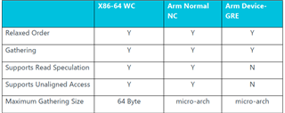
    • The memset/memcpy operations in user space are memory operations, but the compiler and CPU are unaware that this is an I/O memory space. They might perform clever reordering operations, but could this operation cause byte enable confusion? Perhaps adding a memory barrier might improve the situation? I don't have a PCIe protocol analyzer to see what happened. If it's convenient for you, could you take a look?

    • It is unclear whether the PCIe module of TDA4 supports the ARM SIMD instruction set. Because in GDB, it can be clearly seen that a Bus error occurs when the 'q0' register writes into the PCIe space.

    // SPDX-License-Identifier: GPL-2.0
    /*
     * Device Tree Source for J721E SoC Family Main Domain peripherals
     *
     * Copyright (C) 2016-2019 Texas Instruments Incorporated - http://www.ti.com/
     */
    #include <dt-bindings/phy/phy.h>
    #include <dt-bindings/mux/mux.h>
    #include <dt-bindings/mux/mux-j721e-wiz.h>
    
    #include <dt-bindings/phy/phy.h>
    
    #if 0
    #define YC_TEST_NO_CAN
    #endif
    &cbass_main {
    	msmc_ram: sram@70000000 {
    		compatible = "mmio-sram";
    		reg = <0x0 0x70000000 0x0 0x800000>;
    		#address-cells = <1>;
    		#size-cells = <1>;
    		ranges = <0x0 0x0 0x70000000 0x800000>;
    
    		atf-sram@0 {
    			reg = <0x0 0x20000>;
    		};
    	};
    
    	scm_conf: scm_conf@100000 {
    		compatible = "syscon", "simple-mfd";
    		reg = <0 0x00100000 0 0x1c000>;
    		#address-cells = <1>;
    		#size-cells = <1>;
    		ranges = <0x0 0x0 0x00100000 0x1c000>;
    
    		pcie0_ctrl: pcie-ctrl@4070 {
    			compatible = "syscon";
    			reg = <0x00004070 0x4>;
    		};
    
    		pcie1_ctrl: pcie-ctrl@4074 {
    			compatible = "syscon";
    			reg = <0x00004074 0x4>;
    		};
    
    		pcie2_ctrl: pcie-ctrl@4078 {
    			compatible = "syscon";
    			reg = <0x00004078 0x4>;
    		};
    
    		pcie3_ctrl: pcie-ctrl@407c {
    			compatible = "syscon";
    			reg = <0x0000407c 0x4>;
    		};
    		/******Board A & B******/
    		serdes_ln_ctrl: serdes_ln_ctrl@4080 {
    			compatible = "mmio-mux";
    			#mux-control-cells = <1>;
    			mux-reg-masks = <0x4090 0x3>, <0x4094 0x3>, /* SERDES1 lane0/1 select */
    					<0x40a0 0x3>, <0x40a4 0x3>, /* SERDES2 lane0/1 select */
    					<0x40b0 0x3>, <0x40b4 0x3>, /* SERDES3 lane0/1 select */
    					<0x40c0 0x3>, <0x40c4 0x3>, <0x40c8 0x3>, <0x40cc 0x3>;
    					/* SERDES4 lane1/2/3 select */
    			idle-states = <SERDES1_LANE0_PCIE1_LANE0>, <SERDES1_LANE1_PCIE1_LANE1>,
    				      <SERDES2_LANE0_PCIE2_LANE0>, <SERDES2_LANE1_PCIE2_LANE1>,
    				      <MUX_IDLE_AS_IS>, <SERDES3_LANE1_USB3_0>,
    				      <SERDES4_LANE0_EDP_LANE0>, <SERDES4_LANE1_EDP_LANE1>, <SERDES4_LANE2_EDP_LANE2>, <SERDES4_LANE3_EDP_LANE3>;
    		};
    
    		usb_serdes_mux: mux-controller@4000 {
    			compatible = "mmio-mux";
    			#mux-control-cells = <1>;
    			mux-reg-masks = <0x4000 0x8000000>, /* USB0 to SERDES0/3 mux */
    					<0x4010 0x8000000>; /* USB1 to SERDES1/2 mux */
    	    };
    	};
    
    	gic500: interrupt-controller@1800000 {
    		compatible = "arm,gic-v3";
    		#address-cells = <2>;
    		#size-cells = <2>;
    		ranges;
    		#interrupt-cells = <3>;
    		interrupt-controller;
    		reg = <0x00 0x01800000 0x00 0x10000>,	/* GICD */
    		      <0x00 0x01900000 0x00 0x100000>;	/* GICR */
    
    		/* vcpumntirq: virtual CPU interface maintenance interrupt */
    		interrupts = <GIC_PPI 9 IRQ_TYPE_LEVEL_HIGH>;
    
    		gic_its: gic-its@1820000 {
    			compatible = "arm,gic-v3-its";
    			reg = <0x00 0x01820000 0x00 0x10000>;
    			socionext,synquacer-pre-its = <0x1000000 0x400000>;
    			msi-controller;
    			#msi-cells = <1>;
    		};
    	};
    
    	main_gpio_intr: interrupt-controller0 {
    		compatible = "ti,sci-intr";
    		ti,intr-trigger-type = <1>;
    		interrupt-controller;
    		interrupt-parent = <&gic500>;
    		#interrupt-cells = <1>;
    		ti,sci = <&dmsc>;
    		ti,sci-dev-id = <131>;
    		ti,interrupt-ranges = <8 392 56>;
    	};
    
    	cbass_main_navss: navss@30000000 {
    		compatible = "simple-mfd";
    		#address-cells = <2>;
    		#size-cells = <2>;
    		ranges;
    		dma-coherent;
    		dma-ranges;
    
    		ti,sci-dev-id = <199>;
    
    		main_navss_intr: interrupt-controller1 {
    			compatible = "ti,sci-intr";
    			ti,intr-trigger-type = <4>;
    			interrupt-controller;
    			interrupt-parent = <&gic500>;
    			#interrupt-cells = <1>;
    			ti,sci = <&dmsc>;
    			ti,sci-dev-id = <213>;
    			ti,interrupt-ranges = <0 64 64>,
    					      <64 448 64>,
    					      <128 672 64>;
    		};
    
    		main_udmass_inta: interrupt-controller@33d00000 {
    			compatible = "ti,sci-inta";
    			reg = <0x0 0x33d00000 0x0 0x100000>;
    			interrupt-controller;
    			interrupt-parent = <&main_navss_intr>;
    			msi-controller;
    			ti,sci = <&dmsc>;
    			ti,sci-dev-id = <209>;
    			ti,interrupt-ranges = <0 0 256>;
    		};
    
    		secure_proxy_main: mailbox@32c00000 {
    			compatible = "ti,am654-secure-proxy";
    			#mbox-cells = <1>;
    			reg-names = "target_data", "rt", "scfg";
    			reg = <0x00 0x32c00000 0x00 0x100000>,
    			      <0x00 0x32400000 0x00 0x100000>,
    			      <0x00 0x32800000 0x00 0x100000>;
    			interrupt-names = "rx_011";
    			interrupts = <GIC_SPI 37 IRQ_TYPE_LEVEL_HIGH>;
    		};
    
    		smmu0: smmu@36600000 {
    			compatible = "arm,smmu-v3";
    			reg = <0x0 0x36600000 0x0 0x100000>;
    			power-domains = <&k3_pds 229 TI_SCI_PD_EXCLUSIVE>;
    			interrupt-parent = <&gic500>;
    			interrupts = <GIC_SPI 772 IRQ_TYPE_EDGE_RISING>,
    				     <GIC_SPI 768 IRQ_TYPE_EDGE_RISING>;
    			interrupt-names = "eventq", "gerror";
    			#iommu-cells = <1>;
    			dma-coherent;
    		};
    
    		hwspinlock: spinlock@30e00000 {
    			compatible = "ti,am654-hwspinlock";
    			reg = <0x00 0x30e00000 0x00 0x1000>;
    			#hwlock-cells = <1>;
    		};
    
    		mailbox0_cluster0: mailbox@31f80000 {
    			compatible = "ti,am654-mailbox";
    			reg = <0x00 0x31f80000 0x00 0x200>;
    			#mbox-cells = <1>;
    			ti,mbox-num-users = <4>;
    			ti,mbox-num-fifos = <16>;
    			interrupt-parent = <&main_navss_intr>;
    		};
    
    		mailbox0_cluster1: mailbox@31f81000 {
    			compatible = "ti,am654-mailbox";
    			reg = <0x00 0x31f81000 0x00 0x200>;
    			#mbox-cells = <1>;
    			ti,mbox-num-users = <4>;
    			ti,mbox-num-fifos = <16>;
    			interrupt-parent = <&main_navss_intr>;
    		};
    
    		mailbox0_cluster2: mailbox@31f82000 {
    			compatible = "ti,am654-mailbox";
    			reg = <0x00 0x31f82000 0x00 0x200>;
    			#mbox-cells = <1>;
    			ti,mbox-num-users = <4>;
    			ti,mbox-num-fifos = <16>;
    			interrupt-parent = <&main_navss_intr>;
    		};
    
    		mailbox0_cluster3: mailbox@31f83000 {
    			compatible = "ti,am654-mailbox";
    			reg = <0x00 0x31f83000 0x00 0x200>;
    			#mbox-cells = <1>;
    			ti,mbox-num-users = <4>;
    			ti,mbox-num-fifos = <16>;
    			interrupt-parent = <&main_navss_intr>;
    		};
    
    		mailbox0_cluster4: mailbox@31f84000 {
    			compatible = "ti,am654-mailbox";
    			reg = <0x00 0x31f84000 0x00 0x200>;
    			#mbox-cells = <1>;
    			ti,mbox-num-users = <4>;
    			ti,mbox-num-fifos = <16>;
    			interrupt-parent = <&main_navss_intr>;
    		};
    
    		mailbox0_cluster5: mailbox@31f85000 {
    			compatible = "ti,am654-mailbox";
    			reg = <0x00 0x31f85000 0x00 0x200>;
    			#mbox-cells = <1>;
    			ti,mbox-num-users = <4>;
    			ti,mbox-num-fifos = <16>;
    			interrupt-parent = <&main_navss_intr>;
    		};
    
    		mailbox0_cluster6: mailbox@31f86000 {
    			compatible = "ti,am654-mailbox";
    			reg = <0x00 0x31f86000 0x00 0x200>;
    			#mbox-cells = <1>;
    			ti,mbox-num-users = <4>;
    			ti,mbox-num-fifos = <16>;
    			interrupt-parent = <&main_navss_intr>;
    		};
    
    		mailbox0_cluster7: mailbox@31f87000 {
    			compatible = "ti,am654-mailbox";
    			reg = <0x00 0x31f87000 0x00 0x200>;
    			#mbox-cells = <1>;
    			ti,mbox-num-users = <4>;
    			ti,mbox-num-fifos = <16>;
    			interrupt-parent = <&main_navss_intr>;
    		};
    
    		mailbox0_cluster8: mailbox@31f88000 {
    			compatible = "ti,am654-mailbox";
    			reg = <0x00 0x31f88000 0x00 0x200>;
    			#mbox-cells = <1>;
    			ti,mbox-num-users = <4>;
    			ti,mbox-num-fifos = <16>;
    			interrupt-parent = <&main_navss_intr>;
    		};
    
    		mailbox0_cluster9: mailbox@31f89000 {
    			compatible = "ti,am654-mailbox";
    			reg = <0x00 0x31f89000 0x00 0x200>;
    			#mbox-cells = <1>;
    			ti,mbox-num-users = <4>;
    			ti,mbox-num-fifos = <16>;
    			interrupt-parent = <&main_navss_intr>;
    		};
    
    		mailbox0_cluster10: mailbox@31f8a000 {
    			compatible = "ti,am654-mailbox";
    			reg = <0x00 0x31f8a000 0x00 0x200>;
    			#mbox-cells = <1>;
    			ti,mbox-num-users = <4>;
    			ti,mbox-num-fifos = <16>;
    			interrupt-parent = <&main_navss_intr>;
    		};
    
    		mailbox0_cluster11: mailbox@31f8b000 {
    			compatible = "ti,am654-mailbox";
    			reg = <0x00 0x31f8b000 0x00 0x200>;
    			#mbox-cells = <1>;
    			ti,mbox-num-users = <4>;
    			ti,mbox-num-fifos = <16>;
    			interrupt-parent = <&main_navss_intr>;
    		};
    
    		main_ringacc: ringacc@3c000000 {
    			compatible = "ti,am654-navss-ringacc";
    			reg =	<0x0 0x3c000000 0x0 0x400000>,
    				<0x0 0x38000000 0x0 0x400000>,
    				<0x0 0x31120000 0x0 0x100>,
    				<0x0 0x33000000 0x0 0x40000>;
    			reg-names = "rt", "fifos", "proxy_gcfg", "proxy_target";
    			ti,num-rings = <1024>;
    			ti,sci-rm-range-gp-rings = <0x1>; /* GP ring range */
    			ti,sci = <&dmsc>;
    			ti,sci-dev-id = <211>;
    			msi-parent = <&main_udmass_inta>;
    		};
    
    		main_udmap: dma-controller@31150000 {
    			compatible = "ti,j721e-navss-main-udmap";
    			reg =	<0x0 0x31150000 0x0 0x100>,
    				<0x0 0x34000000 0x0 0x100000>,
    				<0x0 0x35000000 0x0 0x100000>;
    			reg-names = "gcfg", "rchanrt", "tchanrt";
    			msi-parent = <&main_udmass_inta>;
    			#dma-cells = <1>;
    
    			ti,sci = <&dmsc>;
    			ti,sci-dev-id = <212>;
    			ti,ringacc = <&main_ringacc>;
    
    			ti,sci-rm-range-tchan = <0x0d>, /* TX_CHAN */
    						<0x0f>, /* TX_HCHAN */
    						<0x10>; /* TX_UHCHAN */
    			ti,sci-rm-range-rchan = <0x0a>, /* RX_CHAN */
    						<0x0b>, /* RX_HCHAN */
    						<0x0c>; /* RX_UHCHAN */
    			ti,sci-rm-range-rflow = <0x00>; /* GP RFLOW */
    		};
    
    		cpts@310d0000 {
    			compatible = "ti,j721e-cpts";
    			reg = <0x0 0x310d0000 0x0 0x400>;
    			reg-names = "cpts";
    			clocks = <&k3_clks 201 1>;
    			clock-names = "cpts";
    			interrupts-extended = <&main_navss_intr 391>;
    			interrupt-names = "cpts";
    			ti,cpts-periodic-outputs = <6>;
    			ti,cpts-ext-ts-inputs = <8>;
    		};
    
    		navss_pat0: pat@31010000 {
    			compatible = "ti,j721e-pat";
    			reg = <0x00 0x31010000 0x00 0x00000100>,
    			      <0x00 0x36400000 0x00 0x00040000>;
    			reg-names = "mmrs",
    				    "table";
    			ti,pat-window-base = <0x48 0x00000000>;
    			ti,pat-window-size = <0x00 0x40000000>;
    		};
    
    		navss_pat1: pat@31011000 {
    			compatible = "ti,j721e-pat";
    			reg = <0x00 0x31011000 0x00 0x00000100>,
    			      <0x00 0x36440000 0x00 0x00040000>;
    			reg-names = "mmrs",
    				    "table";
    			ti,pat-window-base = <0x48 0x40000000>;
    			ti,pat-window-size = <0x00 0x40000000>;
    		};
    
    		navss_pat2: pat@31012000 {
    			compatible = "ti,j721e-pat";
    			reg = <0x00 0x31012000 0x00 0x00000100>,
    			      <0x00 0x36480000 0x00 0x00040000>;
    			reg-names = "mmrs",
    				    "table";
    			ti,pat-window-base = <0x48 0x80000000>;
    			ti,pat-window-size = <0x00 0x40000000>;
    		};
    
    		navss_pat3: pat@31013000 {
    			compatible = "ti,j721e-pat";
    			reg = <0x00 0x31013000 0x00 0x00000100>,
    			      <0x00 0x364C0000 0x00 0x00008000>;
    			reg-names = "mmrs",
    				    "table";
    			ti,pat-window-base = <0x49 0x00000000>;
    			ti,pat-window-size = <0x00 0x80000000>;
    		};
    
    		navss_pat4: pat@31014000 {
    			compatible = "ti,j721e-pat";
    			reg = <0x00 0x31014000 0x00 0x00000100>,
    			      <0x00 0x36500000 0x00 0x00008000>;
    			reg-names = "mmrs",
    				    "table";
    			ti,pat-window-base = <0x49 0x80000000>;
    			ti,pat-window-size = <0x00 0x80000000>;
    		};
    	};
    
    	main_crypto: crypto@4e00000 {
    		compatible = "ti,j721e-sa2ul";
    		reg = <0x0 0x4e00000 0x0 0x1200>;
    		power-domains = <&k3_pds 264 TI_SCI_PD_EXCLUSIVE>;
    		#address-cells = <2>;
    		#size-cells = <2>;
    		ranges = <0x0 0x04e00000 0x00 0x04e00000 0x0 0x30000>;
    
    		status = "okay";
    
    		dmas = <&main_udmap 0xc000>, <&main_udmap 0x4000>,
    				<&main_udmap 0x4001>;
    		dma-names = "tx", "rx1", "rx2";
    		dma-coherent;
    
    		rng: rng@4e10000 {
    			compatible = "inside-secure,safexcel-eip76";
    			reg = <0x0 0x4e10000 0x0 0x7d>;
    			interrupts = <GIC_SPI 11 IRQ_TYPE_LEVEL_HIGH>;
    			clocks = <&k3_clks 264 1>;
    		};
    	};
    
    	main_pmx0: pinmux@11c000 {
    		compatible = "pinctrl-single";
    		/* Proxy 0 addressing */
    		reg = <0x0 0x11c000 0x0 0x2b4>;
    		#pinctrl-cells = <1>;
    		pinctrl-single,register-width = <32>;
    		pinctrl-single,function-mask = <0xffffffff>;
    	};
    
    	dummy_cmn_refclk: dummy_cmn_refclk {
    		#clock-cells = <0>;
    		compatible = "fixed-clock";
    		clock-frequency = <0>;
    	};
    
    	dummy_cmn_refclk1: dummy_cmn_refclk1 {
    		#clock-cells = <0>;
    		compatible = "fixed-clock";
    		clock-frequency = <0>;
    	};
    
    	serdes_wiz0: wiz@5000000 {
    		compatible = "ti,j721e-wiz-16g";
    		#address-cells = <1>;
    		#size-cells = <1>;
    		power-domains = <&k3_pds 292 TI_SCI_PD_EXCLUSIVE>;
    		clocks = <&k3_clks 292 5>, <&k3_clks 292 11>, <&dummy_cmn_refclk>;
    		clock-names = "fck", "core_ref_clk", "ext_ref_clk";
    		assigned-clocks = <&k3_clks 292 11>, <&k3_clks 292 0>;
    		assigned-clock-parents = <&k3_clks 292 15>, <&k3_clks 292 4>;
    		num-lanes = <2>;
    		#reset-cells = <1>;
    		ranges = <0x5000000 0x0 0x5000000 0x10000>;
    
    		wiz0_pll0_refclk: pll0-refclk {
    			clocks = <&k3_clks 292 11>, <&dummy_cmn_refclk>;
    			#clock-cells = <0>;
    			assigned-clocks = <&wiz0_pll0_refclk>;
    			assigned-clock-parents = <&k3_clks 292 11>;
    		};
    
    		wiz0_pll1_refclk: pll1-refclk {
    			clocks = <&k3_clks 292 0>, <&dummy_cmn_refclk1>;
    			#clock-cells = <0>;
    			assigned-clocks = <&wiz0_pll1_refclk>;
    			assigned-clock-parents = <&k3_clks 292 0>;
    		};
    
    		wiz0_refclk_dig: refclk-dig {
    			clocks = <&k3_clks 292 11>, <&k3_clks 292 0>, <&dummy_cmn_refclk>, <&dummy_cmn_refclk1>;
    			#clock-cells = <0>;
    			assigned-clocks = <&wiz0_refclk_dig>;
    			assigned-clock-parents = <&k3_clks 292 11>;
    		};
    
    		wiz0_cmn_refclk_dig_div: cmn-refclk-dig-div {
    			clocks = <&wiz0_refclk_dig>;
    			#clock-cells = <0>;
    		};
    
    		wiz0_cmn_refclk1_dig_div: cmn-refclk1-dig-div {
    			clocks = <&wiz0_pll1_refclk>;
    			#clock-cells = <0>;
    		};
    
    		serdes0: serdes@5000000 {
    			compatible = "ti,sierra-phy-t0";
    			reg-names = "serdes";
    			reg = <0x5000000 0x10000>;
    			#address-cells = <1>;
    			#size-cells = <0>;
    			resets = <&serdes_wiz0 0>;
    			reset-names = "sierra_reset";
    			clocks = <&wiz0_cmn_refclk_dig_div>, <&wiz0_cmn_refclk1_dig_div>;
    			clock-names = "cmn_refclk_dig_div", "cmn_refclk1_dig_div";
    		};
    	};
    
    	serdes_wiz1: wiz@5010000 {
    		compatible = "ti,j721e-wiz-16g";
    		#address-cells = <1>;
    		#size-cells = <1>;
    		power-domains = <&k3_pds 293 TI_SCI_PD_EXCLUSIVE>;
    		clocks = <&k3_clks 293 5>, <&k3_clks 293 13>, <&dummy_cmn_refclk>;
    		clock-names = "fck", "core_ref_clk", "ext_ref_clk";
    		assigned-clocks = <&k3_clks 293 13>, <&k3_clks 293 0>;
    		assigned-clock-parents = <&k3_clks 293 17>, <&k3_clks 293 4>;
    		num-lanes = <2>;
    		#reset-cells = <1>;
    		ranges = <0x5010000 0x0 0x5010000 0x10000>;
    
    		wiz1_pll0_refclk: pll0-refclk {
    			clocks = <&k3_clks 293 13>, <&dummy_cmn_refclk>;
    			#clock-cells = <0>;
    			assigned-clocks = <&wiz1_pll0_refclk>;
    			assigned-clock-parents = <&k3_clks 293 13>;
    		};
    
    		wiz1_pll1_refclk: pll1-refclk {
    			clocks = <&k3_clks 293 0>, <&dummy_cmn_refclk1>;
    			#clock-cells = <0>;
    			assigned-clocks = <&wiz1_pll1_refclk>;
    			assigned-clock-parents = <&k3_clks 293 0>;
    		};
    
    		wiz1_refclk_dig: refclk-dig {
    			clocks = <&k3_clks 293 13>, <&k3_clks 293 0>, <&dummy_cmn_refclk>, <&dummy_cmn_refclk1>;
    			#clock-cells = <0>;
    			assigned-clocks = <&wiz1_refclk_dig>;
    			assigned-clock-parents = <&k3_clks 293 13>;
    		};
    
    		wiz1_cmn_refclk_dig_div: cmn-refclk-dig-div{
    			clocks = <&wiz1_refclk_dig>;
    			#clock-cells = <0>;
    		};
    
    		wiz1_cmn_refclk1_dig_div: cmn-refclk1-dig-div {
    			clocks = <&wiz1_pll1_refclk>;
    			#clock-cells = <0>;
    		};
    
    		serdes1: serdes@5010000 {
    			compatible = "ti,sierra-phy-t0";
    			reg-names = "serdes";
    			reg = <0x5010000 0x10000>;
    			#address-cells = <1>;
    			#size-cells = <0>;
    			resets = <&serdes_wiz1 0>;
    			reset-names = "sierra_reset";
    			clocks = <&wiz1_cmn_refclk_dig_div>, <&wiz1_cmn_refclk1_dig_div>;
    			clock-names = "cmn_refclk_dig_div", "cmn_refclk1_dig_div";
    		};
    	};
    
    	serdes_wiz2: wiz@5020000 {
    		compatible = "ti,j721e-wiz-16g";
    		#address-cells = <1>;
    		#size-cells = <1>;
    		power-domains = <&k3_pds 294 TI_SCI_PD_EXCLUSIVE>;
    		clocks = <&k3_clks 294 5>, <&k3_clks 294 11>, <&dummy_cmn_refclk>;
    		clock-names = "fck", "core_ref_clk", "ext_ref_clk";
    		assigned-clocks = <&k3_clks 294 11>, <&k3_clks 294 0>;
    		assigned-clock-parents = <&k3_clks 294 15>, <&k3_clks 294 4>;
    		num-lanes = <2>;
    		#reset-cells = <1>;
    		ranges = <0x5020000 0x0 0x5020000 0x10000>;
    
    		wiz2_pll0_refclk: pll0-refclk {
    			clocks = <&k3_clks 294 11>, <&dummy_cmn_refclk>;
    			#clock-cells = <0>;
    			assigned-clocks = <&wiz2_pll0_refclk>;
    			assigned-clock-parents = <&k3_clks 294 11>;
    		};
    
    		wiz2_pll1_refclk: pll1-refclk {
    			clocks = <&k3_clks 294 0>, <&dummy_cmn_refclk1>;
    			#clock-cells = <0>;
    			assigned-clocks = <&wiz2_pll1_refclk>;
    			assigned-clock-parents = <&k3_clks 294 0>;
    		};
    
    		wiz2_refclk_dig: refclk-dig {
    			clocks = <&k3_clks 294 11>, <&k3_clks 294 0>, <&dummy_cmn_refclk>, <&dummy_cmn_refclk1>;
    			#clock-cells = <0>;
    			assigned-clocks = <&wiz2_refclk_dig>;
    			assigned-clock-parents = <&k3_clks 294 11>;
    		};
    
    		wiz2_cmn_refclk_dig_div: cmn-refclk-dig-div {
    			clocks = <&wiz2_refclk_dig>;
    			#clock-cells = <0>;
    		};
    
    		wiz2_cmn_refclk1_dig_div: cmn-refclk1-dig-div {
    			clocks = <&wiz2_pll1_refclk>;
    			#clock-cells = <0>;
    		};
    
    		serdes2: serdes@5020000 {
    			compatible = "ti,sierra-phy-t0";
    			reg-names = "serdes";
    			reg = <0x5020000 0x10000>;
    			#address-cells = <1>;
    			#size-cells = <0>;
    			resets = <&serdes_wiz2 0>;
    			reset-names = "sierra_reset";
    			clocks = <&wiz2_cmn_refclk_dig_div>, <&wiz2_cmn_refclk1_dig_div>;
    			clock-names = "cmn_refclk_dig_div", "cmn_refclk1_dig_div";
    		};
    	};
    
    	serdes_wiz3: wiz@5030000 {
    		compatible = "ti,j721e-wiz-16g";
    		#address-cells = <1>;
    		#size-cells = <1>;
    		power-domains = <&k3_pds 295 TI_SCI_PD_EXCLUSIVE>;
    		clocks = <&k3_clks 295 5>, <&k3_clks 295 9>, <&dummy_cmn_refclk>;
    		clock-names = "fck", "core_ref_clk", "ext_ref_clk";
    		assigned-clocks = <&k3_clks 295 9>, <&k3_clks 295 0>;
    		assigned-clock-parents = <&k3_clks 295 13>, <&k3_clks 295 4>;
    		num-lanes = <2>;
    		#reset-cells = <1>;
    		ranges = <0x5030000 0x0 0x5030000 0x10000>;
    
    		wiz3_pll0_refclk: pll0-refclk {
    			clocks = <&k3_clks 295 9>, <&dummy_cmn_refclk>;
    			#clock-cells = <0>;
    			assigned-clocks = <&wiz3_pll0_refclk>;
    			assigned-clock-parents = <&k3_clks 295 9>;
    		};
    
    		wiz3_pll1_refclk: pll1-refclk {
    			clocks = <&k3_clks 295 0>, <&dummy_cmn_refclk1>;
    			#clock-cells = <0>;
    			assigned-clocks = <&wiz3_pll1_refclk>;
    			assigned-clock-parents = <&k3_clks 295 0>;
    		};
    
    		wiz3_refclk_dig: refclk-dig {
    			clocks = <&k3_clks 295 9>, <&k3_clks 295 0>, <&dummy_cmn_refclk>, <&dummy_cmn_refclk1>;
    			#clock-cells = <0>;
    			assigned-clocks = <&wiz3_refclk_dig>;
    			assigned-clock-parents = <&k3_clks 295 9>;
    		};
    
    		wiz3_cmn_refclk_dig_div: cmn-refclk-dig-div {
    			clocks = <&wiz3_refclk_dig>;
    			#clock-cells = <0>;
    		};
    
    		wiz3_cmn_refclk1_dig_div: cmn-refclk1-dig-div {
    			clocks = <&wiz3_pll1_refclk>;
    			#clock-cells = <0>;
    		};
    
    		serdes3: serdes@5030000 {
    			compatible = "ti,sierra-phy-t0";
    			reg-names = "serdes";
    			reg = <0x5030000 0x10000>;
    			#address-cells = <1>;
    			#size-cells = <0>;
    			resets = <&serdes_wiz3 0>;
    			reset-names = "sierra_reset";
    			clocks = <&wiz3_cmn_refclk_dig_div>, <&wiz3_cmn_refclk1_dig_div>;
    			clock-names = "cmn_refclk_dig_div", "cmn_refclk1_dig_div";
    		};
    	};
    
    	pcie0_rc: pcie@2900000 {
    		compatible = "ti,j721e-pcie-host";
    		reg = <0x00 0x02900000 0x00 0x1000>,
    		      <0x00 0x02907000 0x00 0x400>,
    		      <0x00 0x0d000000 0x00 0x00800000>,
    		      <0x00 0x10000000 0x00 0x00001000>;
    		reg-names = "intd_cfg", "user_cfg", "reg", "cfg";
    		ti,syscon-pcie-ctrl = <&pcie0_ctrl>;
    		max-link-speed = <3>;
    		num-lanes = <2>;
    		power-domains = <&k3_pds 239 TI_SCI_PD_EXCLUSIVE>;
    		clocks = <&k3_clks 239 1>;
    		clock-names = "fck";
    		#address-cells = <3>;
    		#size-cells = <2>;
    		bus-range = <0x0 0xf>;
    		cdns,max-outbound-regions = <32>;
    		cdns,no-bar-match-nbits = <64>;
    		vendor-id = /bits/ 16 <0x104c>;
    		device-id = /bits/ 16 <0xb00d>;
    		msi-map = <0x0 &gic_its 0x0 0x10000>;
    		dma-coherent;
    		ranges = <0x01000000 0x0 0x10001000  0x00 0x10001000  0x0 0x0010000>,
    			 <0x02000000 0x0 0x10011000  0x00 0x10011000  0x0 0x7fef000>;
    		#interrupt-cells = <1>;
    		interrupt-map-mask = <0 0 0 7>;
    		interrupt-map = <0 0 0 1 &pcie0_intc 0>, /* INT A */
    				<0 0 0 2 &pcie0_intc 0>, /* INT B */
    				<0 0 0 3 &pcie0_intc 0>, /* INT C */
    				<0 0 0 4 &pcie0_intc 0>; /* INT D */
    
    		pcie0_intc: legacy-interrupt-controller {
    			interrupt-controller;
    			#interrupt-cells = <1>;
    			interrupt-parent = <&gic500>;
    			interrupts = <GIC_SPI 312 IRQ_TYPE_EDGE_RISING>;
    		};
    	};
    
    	pcie0_ep: pcie-ep@2900000 {
    		compatible = "ti,j721e-pcie-ep";
    		reg = <0x00 0x02900000 0x00 0x1000>,
    		      <0x00 0x02907000 0x00 0x400>,
    		      <0x00 0x0d000000 0x00 0x00800000>,
    		      <0x00 0x10000000 0x00 0x08000000>;
    		reg-names = "intd_cfg", "user_cfg", "reg", "mem";
    		ti,syscon-pcie-ctrl = <&pcie0_ctrl>;
    		max-link-speed = <3>;
    		num-lanes = <2>;
    		power-domains = <&k3_pds 239 TI_SCI_PD_EXCLUSIVE>;
    		clocks = <&k3_clks 239 1>;
    		clock-names = "fck";
    		cdns,max-outbound-regions = <32>;
    		max-functions = /bits/ 8 <6>;
    		max-virtual-functions = /bits/ 16 <4 4 4 4 0 0>;
    		dma-coherent;
    		#address-cells = <2>;
    		#size-cells = <2>;
    		ranges;
    	};
    
    	pcie1_rc: pcie@2910000 {
    		compatible = "ti,j721e-pcie-host";
    		reg = <0x00 0x02910000 0x00 0x1000>,
    		      <0x00 0x02917000 0x00 0x400>,
    		      <0x00 0x0d800000 0x00 0x00800000>,
    		      <0x41 0x00000000 0x00 0x00001000>;
    		reg-names = "intd_cfg", "user_cfg", "reg", "cfg";
    		ti,syscon-pcie-ctrl = <&pcie1_ctrl>;
    		max-link-speed = <3>;
    		num-lanes = <2>;
    		power-domains = <&k3_pds 240 TI_SCI_PD_EXCLUSIVE>;
    		clocks = <&k3_clks 240 1>;
    		clock-names = "fck";
    		#address-cells = <3>;
    		#size-cells = <2>;
    		bus-range = <0x0 0xf>;
    		cdns,max-outbound-regions = <32>;
    		cdns,no-bar-match-nbits = <64>;
    		vendor-id = /bits/ 16 <0x104c>;
    		device-id = /bits/ 16 <0xb00d>;
    		msi-map = <0x0 &gic_its 0x10000 0x10000>;
    		dma-coherent;
    		ranges = <0x01000000 0x00 0x00001000  0x41 0x00001000  0x0 0x0010000>,
    			 <0x02000000 0x00 0x00011000  0x41 0x00011000  0x0 0xfffef000>;
    		#interrupt-cells = <1>;
    		interrupt-map-mask = <0 0 0 7>;
    		interrupt-map = <0 0 0 1 &pcie1_intc 0>, /* INT A */
    				<0 0 0 2 &pcie1_intc 0>, /* INT B */
    				<0 0 0 3 &pcie1_intc 0>, /* INT C */
    				<0 0 0 4 &pcie1_intc 0>; /* INT D */
    
    		pcie1_intc: legacy-interrupt-controller {
    			interrupt-controller;
    			#interrupt-cells = <2>;
    			interrupt-parent = <&gic500>;
    			interrupts = <GIC_SPI 324 IRQ_TYPE_EDGE_RISING>;
    		};
    	};
    
    	pcie1_ep: pcie-ep@2910000 {
    		compatible = "ti,j721e-pcie-ep";
    		reg = <0x00 0x02910000 0x00 0x1000>,
    		      <0x00 0x02917000 0x00 0x400>,
    		      <0x00 0x0d800000 0x00 0x00800000>,
    		      <0x00 0x18000000 0x00 0x08000000>;
    		reg-names = "intd_cfg", "user_cfg", "reg", "mem";
    		ti,syscon-pcie-ctrl = <&pcie1_ctrl>;
    		max-link-speed = <3>;
    		num-lanes = <2>;
    		power-domains = <&k3_pds 240 TI_SCI_PD_EXCLUSIVE>;
    		clocks = <&k3_clks 240 1>;
    		clock-names = "fck";
    		cdns,max-outbound-regions = <32>;
    		max-functions = /bits/ 8 <6>;
    		max-virtual-functions = /bits/ 16 <4 4 4 4 0 0>;
    		dma-coherent;
    	};
    
    	pcie2_rc: pcie@2920000 {
    		compatible = "ti,j721e-pcie-host";
    		reg = <0x00 0x02920000 0x00 0x1000>,
    		      <0x00 0x02927000 0x00 0x400>,
    		      <0x00 0x0e000000 0x00 0x00800000>,
    		      <0x44 0x00000000 0x00 0x00001000>;
    		reg-names = "intd_cfg", "user_cfg", "reg", "cfg";
    		ti,syscon-pcie-ctrl = <&pcie2_ctrl>;
    		max-link-speed = <3>;
    		num-lanes = <2>;
    		power-domains = <&k3_pds 241 TI_SCI_PD_EXCLUSIVE>;
    		clocks = <&k3_clks 241 1>;
    		clock-names = "fck";
    		#address-cells = <3>;
    		#size-cells = <2>;
    		bus-range = <0x0 0xf>;
    		cdns,max-outbound-regions = <32>;
    		cdns,no-bar-match-nbits = <64>;
    		vendor-id = /bits/ 16 <0x104c>;
    		device-id = /bits/ 16 <0xb00d>;
    		msi-map = <0x0 &gic_its 0x20000 0x10000>;
    		dma-coherent;
    		ranges = <0x01000000 0x00 0x00001000  0x44 0x00001000  0x0 0x0010000>,
    			 <0x02000000 0x00 0x00011000  0x44 0x00011000  0x0 0x7fef000>;
    		#interrupt-cells = <1>;
    		interrupt-map-mask = <0 0 0 7>;
    		interrupt-map = <0 0 0 1 &pcie2_intc 0>, /* INT A */
    				<0 0 0 2 &pcie2_intc 0>, /* INT B */
    				<0 0 0 3 &pcie2_intc 0>, /* INT C */
    				<0 0 0 4 &pcie2_intc 0>; /* INT D */
    
    		pcie2_intc: legacy-interrupt-controller {
    			interrupt-controller;
    			#interrupt-cells = <2>;
    			interrupt-parent = <&gic500>;
    			interrupts = <GIC_SPI 336 IRQ_TYPE_EDGE_RISING>;
    		};
    	};
    
    	pcie2_ep: pcie-ep@2920000 {
    		compatible = "ti,j721e-pcie-ep";
    		reg = <0x00 0x02920000 0x00 0x1000>,
    		      <0x00 0x02927000 0x00 0x400>,
    		      <0x00 0x0e000000 0x00 0x00800000>,
    		      <0x44 0x00000000 0x00 0x08000000>;
    		reg-names = "intd_cfg", "user_cfg", "reg", "mem";
    		ti,syscon-pcie-ctrl = <&pcie2_ctrl>;
    		max-link-speed = <3>;
    		num-lanes = <2>;
    		power-domains = <&k3_pds 241 TI_SCI_PD_EXCLUSIVE>;
    		clocks = <&k3_clks 241 1>;
    		clock-names = "fck";
    		cdns,max-outbound-regions = <32>;
    		max-functions = /bits/ 8 <6>;
    		max-virtual-functions = /bits/ 16 <4 4 4 4 0 0>;
    		dma-coherent;
    	};
    
    	pcie3_rc: pcie@2930000 {
    		compatible = "ti,j721e-pcie-host";
    		reg = <0x00 0x02930000 0x00 0x1000>,
    		      <0x00 0x02937000 0x00 0x400>,
    		      <0x00 0x0e800000 0x00 0x00800000>,
    		      <0x44 0x10000000 0x00 0x00001000>;
    		reg-names = "intd_cfg", "user_cfg", "reg", "cfg";
    		ti,syscon-pcie-ctrl = <&pcie3_ctrl>;
    		max-link-speed = <3>;
    		num-lanes = <2>;
    		power-domains = <&k3_pds 242 TI_SCI_PD_EXCLUSIVE>;
    		clocks = <&k3_clks 242 1>;
    		clock-names = "fck";
    		#address-cells = <3>;
    		#size-cells = <2>;
    		bus-range = <0x0 0xf>;
    		cdns,max-outbound-regions = <32>;
    		cdns,no-bar-match-nbits = <64>;
    		vendor-id = /bits/ 16 <0x104c>;
    		device-id = /bits/ 16 <0xb00d>;
    		msi-map = <0x0 &gic_its 0x30000 0x10000>;
    		dma-coherent;
    		ranges = <0x01000000 0x00 0x00001000  0x44 0x10001000  0x0 0x0010000>,
    			 <0x02000000 0x00 0x00011000  0x44 0x10011000  0x0 0x7fef000>;
    		#interrupt-cells = <1>;
    		interrupt-map-mask = <0 0 0 7>;
    		interrupt-map = <0 0 0 1 &pcie3_intc 0>, /* INT A */
    				<0 0 0 2 &pcie3_intc 0>, /* INT B */
    				<0 0 0 3 &pcie3_intc 0>, /* INT C */
    				<0 0 0 4 &pcie3_intc 0>; /* INT D */
    
    		pcie3_intc: legacy-interrupt-controller {
    			interrupt-controller;
    			#interrupt-cells = <2>;
    			interrupt-parent = <&gic500>;
    			interrupts = <GIC_SPI 348 IRQ_TYPE_EDGE_RISING>;
    		};
    	};
    
    	pcie3_ep: pcie-ep@2930000 {
    		compatible = "ti,j721e-pcie-ep";
    		reg = <0x00 0x02930000 0x00 0x1000>,
    		      <0x00 0x02937000 0x00 0x400>,
    		      <0x00 0x0e800000 0x00 0x00800000>,
    		      <0x44 0x10000000 0x00 0x08000000>;
    		reg-names = "intd_cfg", "user_cfg", "reg", "mem";
    		ti,syscon-pcie-ctrl = <&pcie3_ctrl>;
    		max-link-speed = <3>;
    		num-lanes = <2>;
    		power-domains = <&k3_pds 242 TI_SCI_PD_EXCLUSIVE>;
    		clocks = <&k3_clks 242 1>;
    		clock-names = "fck";
    		cdns,max-outbound-regions = <32>;
    		max-functions = /bits/ 8 <6>;
    		max-virtual-functions = /bits/ 16 <4 4 4 4 0 0>;
    		dma-coherent;
    		#address-cells = <2>;
    		#size-cells = <2>;
    	};
    
    	serdes_wiz4: wiz@5050000 {
    		compatible = "ti,j721e-wiz-10g";
    		#address-cells = <2>;
    		#size-cells = <2>;
    		power-domains = <&k3_pds 297 TI_SCI_PD_EXCLUSIVE>;
    		clocks = <&k3_clks 297 1>, <&k3_clks 297 9>, <&dummy_cmn_refclk>;
    		clock-names = "fck", "core_ref_clk", "ext_ref_clk";
    		num-lanes = <4>;
    		#reset-cells = <1>;
    		ranges;
    
    		assigned-clocks = <&k3_clks 297 9>;
    		assigned-clock-parents = <&k3_clks 297 10>;
    		assigned-clock-rates = <19200000>;
    
    		wiz4_pll0_refclk: pll0-refclk {
    			clocks = <&k3_clks 297 9>, <&dummy_cmn_refclk>;
    			clock-output-names = "wiz4_pll0_refclk";
    			#clock-cells = <0>;
    			assigned-clocks = <&wiz4_pll0_refclk>;
    			assigned-clock-parents = <&k3_clks 297 9>;
    		};
    
    		wiz4_pll1_refclk: pll1-refclk {
    			clocks = <&k3_clks 297 9>, <&dummy_cmn_refclk>;
    			clock-output-names = "wiz4_pll1_refclk";
    			#clock-cells = <0>;
    			assigned-clocks = <&wiz4_pll1_refclk>;
    			assigned-clock-parents = <&k3_clks 297 9>;
    		};
    
    		wiz4_refclk_dig: refclk-dig {
    			clocks = <&k3_clks 297 9>, <&dummy_cmn_refclk>;
    			clock-output-names = "wiz4_refclk_dig";
    			#clock-cells = <0>;
    			assigned-clocks = <&wiz4_refclk_dig>;
    			assigned-clock-parents = <&k3_clks 297 9>;
    		};
    
    		wiz4_cmn_refclk_dig_div: cmn-refclk-dig-div {
    			clocks = <&wiz4_refclk_dig>;
    			#clock-cells = <0>;
    		};
    
    		wiz4_cmn_refclk1_dig_div: cmn-refclk1-dig-div {
    			clocks = <&wiz4_pll1_refclk>;
    			#clock-cells = <0>;
    		};
    
    		serdes4: serdes@5050000 {
    			/* XXX we also map EDP0 registers here as the PHY driver needs those... */
    			compatible = "ti,j721e-serdes-10g";
    			reg = <0x00 0x05050000 0x0 0x00010000>, /* SERDES_10G0 */
    			      <0x00 0x0A030A00 0x0 0x00000040>; /* DSS_EDP0_V2A_CORE_VP_REGS_APB + 30A00 */
    
    			resets = <&serdes_wiz4 0>;
    			reset-names = "torrent_reset";
    			clocks = <&wiz4_pll0_refclk>;
    			clock-names = "refclk";
    			#address-cells = <1>;
    			#size-cells = <0>;
    			torrent_phy_dp: link@0{
    				reg = <0>;
    				resets = <&serdes_wiz4 1>;
    				cdns,phy-type = <PHY_TYPE_DP>;
    				cdns,num-lanes = <4>;
    				cdns,max-bit-rate = <5400>;
    				#phy-cells = <0>;
    			};
    		};
    	};
    
    	mhdp: dp-bridge@000A000000 {
    		compatible = "ti,j721e-mhdp8546", "cdns,mhdp8546";
    		reg = <0x00 0x0A000000 0x0 0x30A00>, /* DSS_EDP0_V2A_CORE_VP_REGS_APB - upto PHY mapped area */
    		      <0x00 0x04F40000 0x0 0x20>;    /* DSS_EDP0_INTG_CFG_VP */
    
    		status = "disabled";
    
    		clocks = <&k3_clks 151 36>;
    
    		phys = <&torrent_phy_dp>;
    		phy-names = "dpphy";
    
    		interrupt-parent = <&gic500>;
    		interrupts = <GIC_SPI 614 IRQ_TYPE_LEVEL_HIGH>;
    
    		power-domains = <&k3_pds 151 TI_SCI_PD_EXCLUSIVE>;
    
    		/* TODO: No audio config yet */
    
    		dp0_ports: ports {
    			#address-cells = <1>;
    			#size-cells = <0>;
    		};
    	};
    
    	main_uart0: serial@2800000 {
    		compatible = "ti,j721e-uart", "ti,am654-uart";
    		reg = <0x00 0x02800000 0x00 0x100>;
    		reg-shift = <2>;
    		reg-io-width = <4>;
    		interrupts = <GIC_SPI 192 IRQ_TYPE_LEVEL_HIGH>;
    		clock-frequency = <48000000>;
    		current-speed = <115200>;
    		power-domains = <&k3_pds 146 TI_SCI_PD_EXCLUSIVE>;
    		clocks = <&k3_clks 146 0>;
    		clock-names = "fclk";
    	};
    
    	main_uart1: serial@2810000 {
    		compatible = "ti,j721e-uart", "ti,am654-uart";
    		reg = <0x00 0x02810000 0x00 0x100>;
    		reg-shift = <2>;
    		reg-io-width = <4>;
    		interrupts = <GIC_SPI 193 IRQ_TYPE_LEVEL_HIGH>;
    		clock-frequency = <48000000>;
    		current-speed = <115200>;
    		power-domains = <&k3_pds 278 TI_SCI_PD_EXCLUSIVE>;
    		clocks = <&k3_clks 278 0>;
    		clock-names = "fclk";
    	};
    
    	main_uart2: serial@2820000 {
    		compatible = "ti,j721e-uart", "ti,am654-uart";
    		reg = <0x00 0x02820000 0x00 0x100>;
    		reg-shift = <2>;
    		reg-io-width = <4>;
    		interrupts = <GIC_SPI 194 IRQ_TYPE_LEVEL_HIGH>;
    		clock-frequency = <48000000>;
    		current-speed = <115200>;
    		power-domains = <&k3_pds 279 TI_SCI_PD_EXCLUSIVE>;
    		clocks = <&k3_clks 279 0>;
    		clock-names = "fclk";
    	};
    
    	main_uart3: serial@2830000 {
    		compatible = "ti,j721e-uart", "ti,am654-uart";
    		reg = <0x00 0x02830000 0x00 0x100>;
    		reg-shift = <2>;
    		reg-io-width = <4>;
    		interrupts = <GIC_SPI 195 IRQ_TYPE_LEVEL_HIGH>;
    		clock-frequency = <48000000>;
    		current-speed = <115200>;
    		power-domains = <&k3_pds 280 TI_SCI_PD_EXCLUSIVE>;
    		clocks = <&k3_clks 280 0>;
    		clock-names = "fclk";
    	};
    
    	main_uart4: serial@2840000 {
    		compatible = "ti,j721e-uart", "ti,am654-uart";
    		reg = <0x00 0x02840000 0x00 0x100>;
    		reg-shift = <2>;
    		reg-io-width = <4>;
    		interrupts = <GIC_SPI 196 IRQ_TYPE_LEVEL_HIGH>;
    		clock-frequency = <48000000>;
    		current-speed = <115200>;
    		power-domains = <&k3_pds 281 TI_SCI_PD_EXCLUSIVE>;
    		clocks = <&k3_clks 281 0>;
    		clock-names = "fclk";
    	};
    
    	main_uart5: serial@2850000 {
    		compatible = "ti,j721e-uart", "ti,am654-uart";
    		reg = <0x00 0x02850000 0x00 0x100>;
    		reg-shift = <2>;
    		reg-io-width = <4>;
    		interrupts = <GIC_SPI 197 IRQ_TYPE_LEVEL_HIGH>;
    		clock-frequency = <48000000>;
    		current-speed = <115200>;
    		power-domains = <&k3_pds 282 TI_SCI_PD_EXCLUSIVE>;
    		clocks = <&k3_clks 282 0>;
    		clock-names = "fclk";
    	};
    
    	main_uart6: serial@2860000 {
    		compatible = "ti,j721e-uart", "ti,am654-uart";
    		reg = <0x00 0x02860000 0x00 0x100>;
    		reg-shift = <2>;
    		reg-io-width = <4>;
    		interrupts = <GIC_SPI 198 IRQ_TYPE_LEVEL_HIGH>;
    		clock-frequency = <48000000>;
    		current-speed = <115200>;
    		power-domains = <&k3_pds 283 TI_SCI_PD_EXCLUSIVE>;
    		clocks = <&k3_clks 283 0>;
    		clock-names = "fclk";
    	};
    
    	main_uart7: serial@2870000 {
    		compatible = "ti,j721e-uart", "ti,am654-uart";
    		reg = <0x00 0x02870000 0x00 0x100>;
    		reg-shift = <2>;
    		reg-io-width = <4>;
    		interrupts = <GIC_SPI 199 IRQ_TYPE_LEVEL_HIGH>;
    		clock-frequency = <48000000>;
    		current-speed = <115200>;
    		power-domains = <&k3_pds 284 TI_SCI_PD_EXCLUSIVE>;
    		clocks = <&k3_clks 284 0>;
    		clock-names = "fclk";
    	};
    
    	main_uart8: serial@2880000 {
    		compatible = "ti,j721e-uart", "ti,am654-uart";
    		reg = <0x00 0x02880000 0x00 0x100>;
    		reg-shift = <2>;
    		reg-io-width = <4>;
    		interrupts = <GIC_SPI 248 IRQ_TYPE_LEVEL_HIGH>;
    		clock-frequency = <48000000>;
    		current-speed = <115200>;
    		power-domains = <&k3_pds 285 TI_SCI_PD_EXCLUSIVE>;
    		clocks = <&k3_clks 285 0>;
    		clock-names = "fclk";
    	};
    
    	main_uart9: serial@2890000 {
    		compatible = "ti,j721e-uart", "ti,am654-uart";
    		reg = <0x00 0x02890000 0x00 0x100>;
    		reg-shift = <2>;
    		reg-io-width = <4>;
    		interrupts = <GIC_SPI 249 IRQ_TYPE_LEVEL_HIGH>;
    		clock-frequency = <48000000>;
    		current-speed = <115200>;
    		power-domains = <&k3_pds 286 TI_SCI_PD_EXCLUSIVE>;
    		clocks = <&k3_clks 286 0>;
    		clock-names = "fclk";
    	};
    
    	main_gpio0: gpio@600000 {
    		compatible = "ti,j721e-gpio", "ti,keystone-gpio";
    		reg = <0x0 0x00600000 0x0 0x100>;
    		gpio-controller;
    		#gpio-cells = <2>;
    		interrupt-parent = <&main_gpio_intr>;
    		interrupts = <256>, <257>, <258>, <259>,
    			     <260>, <261>, <262>, <263>;
    		interrupt-controller;
    		#interrupt-cells = <2>;
    		ti,ngpio = <128>;
    		ti,davinci-gpio-unbanked = <0>;
    		power-domains = <&k3_pds 105 TI_SCI_PD_EXCLUSIVE>;
    		clocks = <&k3_clks 105 0>;
    		clock-names = "gpio";
    	};
    
    	main_gpio1: gpio@601000 {
    		compatible = "ti,j721e-gpio", "ti,keystone-gpio";
    		reg = <0x0 0x00601000 0x0 0x100>;
    		gpio-controller;
    		#gpio-cells = <2>;
    		interrupt-parent = <&main_gpio_intr>;
    		interrupts = <288>, <289>, <290>;
    		interrupt-controller;
    		#interrupt-cells = <2>;
    		ti,ngpio = <36>;
    		ti,davinci-gpio-unbanked = <0>;
    		power-domains = <&k3_pds 106 TI_SCI_PD_EXCLUSIVE>;
    		clocks = <&k3_clks 106 0>;
    		clock-names = "gpio";
    	};
    
    	main_gpio2: gpio@610000 {
    		compatible = "ti,j721e-gpio", "ti,keystone-gpio";
    		reg = <0x0 0x00610000 0x0 0x100>;
    		gpio-controller;
    		#gpio-cells = <2>;
    		interrupt-parent = <&main_gpio_intr>;
    		interrupts = <264>, <265>, <266>, <267>,
    			     <268>, <269>, <270>, <271>;
    		interrupt-controller;
    		#interrupt-cells = <2>;
    		ti,ngpio = <128>;
    		ti,davinci-gpio-unbanked = <0>;
    		power-domains = <&k3_pds 107 TI_SCI_PD_EXCLUSIVE>;
    		clocks = <&k3_clks 107 0>;
    		clock-names = "gpio";
    	};
    
    	main_gpio3: gpio@611000 {
    		compatible = "ti,j721e-gpio", "ti,keystone-gpio";
    		reg = <0x0 0x00611000 0x0 0x100>;
    		gpio-controller;
    		#gpio-cells = <2>;
    		interrupt-parent = <&main_gpio_intr>;
    		interrupts = <292>, <293>, <294>;
    		interrupt-controller;
    		#interrupt-cells = <2>;
    		ti,ngpio = <36>;
    		ti,davinci-gpio-unbanked = <0>;
    		power-domains = <&k3_pds 108 TI_SCI_PD_EXCLUSIVE>;
    		clocks = <&k3_clks 108 0>;
    		clock-names = "gpio";
    	};
    
    	main_gpio4: gpio@620000 {
    		compatible = "ti,j721e-gpio", "ti,keystone-gpio";
    		reg = <0x0 0x00620000 0x0 0x100>;
    		gpio-controller;
    		#gpio-cells = <2>;
    		interrupt-parent = <&main_gpio_intr>;
    		interrupts = <272>, <273>, <274>, <275>,
    			     <276>, <277>, <278>, <279>;
    		interrupt-controller;
    		#interrupt-cells = <2>;
    		ti,ngpio = <128>;
    		ti,davinci-gpio-unbanked = <0>;
    		power-domains = <&k3_pds 109 TI_SCI_PD_EXCLUSIVE>;
    		clocks = <&k3_clks 109 0>;
    		clock-names = "gpio";
    	};
    
    	main_gpio5: gpio@621000 {
    		compatible = "ti,j721e-gpio", "ti,keystone-gpio";
    		reg = <0x0 0x00621000 0x0 0x100>;
    		gpio-controller;
    		#gpio-cells = <2>;
    		interrupt-parent = <&main_gpio_intr>;
    		interrupts = <296>, <297>, <298>;
    		interrupt-controller;
    		#interrupt-cells = <2>;
    		ti,ngpio = <36>;
    		ti,davinci-gpio-unbanked = <0>;
    		power-domains = <&k3_pds 110 TI_SCI_PD_EXCLUSIVE>;
    		clocks = <&k3_clks 110 0>;
    		clock-names = "gpio";
    	};
    
    	main_gpio6: gpio@630000 {
    		compatible = "ti,j721e-gpio", "ti,keystone-gpio";
    		reg = <0x0 0x00630000 0x0 0x100>;
    		gpio-controller;
    		#gpio-cells = <2>;
    		interrupt-parent = <&main_gpio_intr>;
    		interrupts = <280>, <281>, <282>, <283>,
    			     <284>, <285>, <286>, <287>;
    		interrupt-controller;
    		#interrupt-cells = <2>;
    		ti,ngpio = <128>;
    		ti,davinci-gpio-unbanked = <0>;
    		power-domains = <&k3_pds 111 TI_SCI_PD_EXCLUSIVE>;
    		clocks = <&k3_clks 111 0>;
    		clock-names = "gpio";
    	};
    
    	main_gpio7: gpio@631000 {
    		compatible = "ti,j721e-gpio", "ti,keystone-gpio";
    		reg = <0x0 0x00631000 0x0 0x100>;
    		gpio-controller;
    		#gpio-cells = <2>;
    		interrupt-parent = <&main_gpio_intr>;
    		interrupts = <300>, <301>, <302>;
    		interrupt-controller;
    		#interrupt-cells = <2>;
    		ti,ngpio = <36>;
    		ti,davinci-gpio-unbanked = <0>;
    		power-domains = <&k3_pds 112 TI_SCI_PD_EXCLUSIVE>;
    		clocks = <&k3_clks 112 0>;
    		clock-names = "gpio";
    	};
    
    	main_rti0: watchdog@2200000 {
    		compatible = "ti,rti-wdt";
    		reg = <0x0 0x2200000 0x0 0x100>;
    		clocks = <&k3_clks 252 1>;
    		power-domains = <&k3_pds 252 TI_SCI_PD_EXCLUSIVE>;
    		assigned-clocks = <&k3_clks 252 1>;
    		assigned-clock-parents = <&k3_clks 252 5>;
    	};
    
    	main_rti1: watchdog@2210000 {
    		compatible = "ti,rti-wdt";
    		reg = <0x0 0x2210000 0x0 0x100>;
    		clocks = <&k3_clks 253 1>;
    		power-domains = <&k3_pds 253 TI_SCI_PD_EXCLUSIVE>;
    		assigned-clocks = <&k3_clks 253 1>;
    		assigned-clock-parents = <&k3_clks 253 5>;
    	};
    
    	main_i2c0: i2c@2000000 {
    		compatible = "ti,j721e-i2c", "ti,omap4-i2c";
    		reg = <0x0 0x2000000 0x0 0x100>;
    		interrupts = <GIC_SPI 200 IRQ_TYPE_LEVEL_HIGH>;
    		#address-cells = <1>;
    		#size-cells = <0>;
    		clock-names = "fck";
    		clocks = <&k3_clks 187 0>;
    		power-domains = <&k3_pds 187 TI_SCI_PD_SHARED>;
    	};
    
    	main_i2c1: i2c@2010000 {
    		compatible = "ti,j721e-i2c", "ti,omap4-i2c";
    		reg = <0x0 0x2010000 0x0 0x100>;
    		interrupts = <GIC_SPI 201 IRQ_TYPE_LEVEL_HIGH>;
    		#address-cells = <1>;
    		#size-cells = <0>;
    		clock-names = "fck";
    		clocks = <&k3_clks 188 0>;
    		power-domains = <&k3_pds 188 TI_SCI_PD_EXCLUSIVE>;
    	};
    
    	main_i2c2: i2c@2020000 {
    		compatible = "ti,j721e-i2c", "ti,omap4-i2c";
    		reg = <0x0 0x2020000 0x0 0x100>;
    		interrupts = <GIC_SPI 202 IRQ_TYPE_LEVEL_HIGH>;
    		#address-cells = <1>;
    		#size-cells = <0>;
    		clock-names = "fck";
    		clocks = <&k3_clks 189 0>;
    		power-domains = <&k3_pds 189 TI_SCI_PD_EXCLUSIVE>;
    	};
    
    	main_i2c3: i2c@2030000 {
    		compatible = "ti,j721e-i2c", "ti,omap4-i2c";
    		reg = <0x0 0x2030000 0x0 0x100>;
    		interrupts = <GIC_SPI 203 IRQ_TYPE_LEVEL_HIGH>;
    		#address-cells = <1>;
    		#size-cells = <0>;
    		clock-names = "fck";
    		clocks = <&k3_clks 190 0>;
    		power-domains = <&k3_pds 190 TI_SCI_PD_EXCLUSIVE>;
    	};
    
    	main_i2c4: i2c@2040000 {
    		compatible = "ti,j721e-i2c", "ti,omap4-i2c";
    		reg = <0x0 0x2040000 0x0 0x100>;
    		interrupts = <GIC_SPI 204 IRQ_TYPE_LEVEL_HIGH>;
    		#address-cells = <1>;
    		#size-cells = <0>;
    		clock-names = "fck";
    		clocks = <&k3_clks 191 0>;
    		power-domains = <&k3_pds 191 TI_SCI_PD_EXCLUSIVE>;
    	};
    
    	main_i2c5: i2c@2050000 {
    		compatible = "ti,j721e-i2c", "ti,omap4-i2c";
    		reg = <0x0 0x2050000 0x0 0x100>;
    		interrupts = <GIC_SPI 205 IRQ_TYPE_LEVEL_HIGH>;
    		#address-cells = <1>;
    		#size-cells = <0>;
    		clock-names = "fck";
    		clocks = <&k3_clks 192 0>;
    		power-domains = <&k3_pds 192 TI_SCI_PD_EXCLUSIVE>;
    	};
    
    	main_i2c6: i2c@2060000 {
    		compatible = "ti,j721e-i2c", "ti,omap4-i2c";
    		reg = <0x0 0x2060000 0x0 0x100>;
    		interrupts = <GIC_SPI 206 IRQ_TYPE_LEVEL_HIGH>;
    		#address-cells = <1>;
    		#size-cells = <0>;
    		clock-names = "fck";
    		clocks = <&k3_clks 193 0>;
    		power-domains = <&k3_pds 193 TI_SCI_PD_EXCLUSIVE>;
    	};
    
    	d5520: video-decoder@4300000 {
    	       /* IMG D5520 driver configuration */
    	       compatible = "img,d5500-vxd";
    	       reg = <0x00 0x04300000 0x00 0x100000>;
    	       power-domains = <&k3_pds 144 TI_SCI_PD_EXCLUSIVE>;
    	       interrupts = <GIC_SPI 180 IRQ_TYPE_LEVEL_HIGH>;
    	};
    
    	vxe384: video-encoder@4200000 {
    		compatible = "img,vxe384";
    		reg = <0x00 0x04200000 0x00 0x100000>;
    		power-domains = <&k3_pds 153 TI_SCI_PD_EXCLUSIVE>;
    		interrupts = <GIC_SPI 181 IRQ_TYPE_LEVEL_HIGH>;
    	};
    
    	ufs_wrapper: ufs-wrapper@4e80000 {
    		compatible = "ti,j721e-ufs";
    		reg = <0x0 0x4e80000 0x0 0x100>;
    		power-domains = <&k3_pds 277 TI_SCI_PD_EXCLUSIVE>;
    		clocks = <&k3_clks 277 1>;
    		assigned-clocks = <&k3_clks 277 1>;
    		assigned-clock-parents = <&k3_clks 277 4>;
    		ranges;
    		#address-cells = <2>;
    		#size-cells = <2>;
    
    		ufs@4e84000 {
    			compatible = "cdns,ufshc-m31-16nm", "jedec,ufs-2.0";
    			reg = <0x0 0x4e84000 0x0 0x10000>;
    			interrupts = <GIC_SPI 17 IRQ_TYPE_LEVEL_HIGH>;
    			freq-table-hz = <250000000 250000000>, <19200000 19200000>, <19200000 19200000>;
    			clocks = <&k3_clks 277 0>, <&k3_clks 277 1>, <&k3_clks 277 1>;
    			clock-names = "core_clk", "phy_clk", "ref_clk";
    			dma-coherent;
    		};
    	};
    
    	gpu: gpu@4e20000000 {
    		compatible = "ti,j721e-pvr", "img,pvr-ge8430";
    		reg = <0x4e 0x20000000 0x00 0x80000>;
    		reg-names = "gpu_regs";
    		interrupts = <GIC_SPI 24 IRQ_TYPE_LEVEL_HIGH>;
    		power-domains = <&k3_pds 125 TI_SCI_PD_EXCLUSIVE>, <&k3_pds 126 TI_SCI_PD_EXCLUSIVE>;
    		power-domain-names = "gpu_0", "gpucore_0";
    		clocks = <&k3_clks 125 0>;
    		clock-names = "ctrl";
    	};
    
    	mcasp0: mcasp@02b00000 {
    		compatible = "ti,am33xx-mcasp-audio";
    		reg = <0x0 0x02b00000 0x0 0x2000>,
    			<0x0 0x02b08000 0x0 0x1000>;
    		reg-names = "mpu","dat";
    		interrupts = <GIC_SPI 544 IRQ_TYPE_LEVEL_HIGH>,
    				<GIC_SPI 545 IRQ_TYPE_LEVEL_HIGH>;
    		interrupt-names = "tx", "rx";
    
    		dmas = <&main_udmap 0xc400>, <&main_udmap 0x4400>;
    		dma-names = "tx", "rx";
    
    		clocks = <&k3_clks 174 1>;
    		clock-names = "fck";
    		power-domains = <&k3_pds 174 TI_SCI_PD_EXCLUSIVE>;
    
    		status = "disabled";
    	};
    
    	mcasp1: mcasp@02b10000 {
    		compatible = "ti,am33xx-mcasp-audio";
    		reg = <0x0 0x02b10000 0x0 0x2000>,
    			<0x0 0x02b18000 0x0 0x1000>;
    		reg-names = "mpu","dat";
    		interrupts = <GIC_SPI 546 IRQ_TYPE_LEVEL_HIGH>,
    				<GIC_SPI 547 IRQ_TYPE_LEVEL_HIGH>;
    		interrupt-names = "tx", "rx";
    
    		dmas = <&main_udmap 0xc401>, <&main_udmap 0x4401>;
    		dma-names = "tx", "rx";
    
    		clocks = <&k3_clks 175 1>;
    		clock-names = "fck";
    		power-domains = <&k3_pds 175 TI_SCI_PD_EXCLUSIVE>;
    
    		status = "disabled";
    	};
    
    	mcasp2: mcasp@02b20000 {
    		compatible = "ti,am33xx-mcasp-audio";
    		reg = <0x0 0x02b20000 0x0 0x2000>,
    			<0x0 0x02b28000 0x0 0x1000>;
    		reg-names = "mpu","dat";
    		interrupts = <GIC_SPI 548 IRQ_TYPE_LEVEL_HIGH>,
    				<GIC_SPI 549 IRQ_TYPE_LEVEL_HIGH>;
    		interrupt-names = "tx", "rx";
    
    		dmas = <&main_udmap 0xc402>, <&main_udmap 0x4402>;
    		dma-names = "tx", "rx";
    
    		clocks = <&k3_clks 176 1>;
    		clock-names = "fck";
    		power-domains = <&k3_pds 176 TI_SCI_PD_EXCLUSIVE>;
    
    		status = "disabled";
    	};
    
    	mcasp3: mcasp@02b30000 {
    		compatible = "ti,am33xx-mcasp-audio";
    		reg = <0x0 0x02b30000 0x0 0x2000>,
    			<0x0 0x02b38000 0x0 0x1000>;
    		reg-names = "mpu","dat";
    		interrupts = <GIC_SPI 550 IRQ_TYPE_LEVEL_HIGH>,
    				<GIC_SPI 551 IRQ_TYPE_LEVEL_HIGH>;
    		interrupt-names = "tx", "rx";
    
    		dmas = <&main_udmap 0xc500>, <&main_udmap 0x4500>;
    		dma-names = "tx", "rx";
    
    		clocks = <&k3_clks 177 1>;
    		clock-names = "fck";
    		power-domains = <&k3_pds 177 TI_SCI_PD_EXCLUSIVE>;
    
    		status = "disabled";
    	};
    
    	mcasp4: mcasp@02b40000 {
    		compatible = "ti,am33xx-mcasp-audio";
    		reg = <0x0 0x02b40000 0x0 0x2000>,
    			<0x0 0x02b48000 0x0 0x1000>;
    		reg-names = "mpu","dat";
    		interrupts = <GIC_SPI 552 IRQ_TYPE_LEVEL_HIGH>,
    				<GIC_SPI 553 IRQ_TYPE_LEVEL_HIGH>;
    		interrupt-names = "tx", "rx";
    
    		dmas = <&main_udmap 0xc501>, <&main_udmap 0x4501>;
    		dma-names = "tx", "rx";
    
    		clocks = <&k3_clks 178 1>;
    		clock-names = "fck";
    		power-domains = <&k3_pds 178 TI_SCI_PD_EXCLUSIVE>;
    
    		status = "disabled";
    	};
    
    	mcasp5: mcasp@02b50000 {
    		compatible = "ti,am33xx-mcasp-audio";
    		reg = <0x0 0x02b50000 0x0 0x2000>,
    			<0x0 0x02b58000 0x0 0x1000>;
    		reg-names = "mpu","dat";
    		interrupts = <GIC_SPI 554 IRQ_TYPE_LEVEL_HIGH>,
    				<GIC_SPI 555 IRQ_TYPE_LEVEL_HIGH>;
    		interrupt-names = "tx", "rx";
    
    		dmas = <&main_udmap 0xc502>, <&main_udmap 0x4502>;
    		dma-names = "tx", "rx";
    
    		clocks = <&k3_clks 179 1>;
    		clock-names = "fck";
    		power-domains = <&k3_pds 179 TI_SCI_PD_EXCLUSIVE>;
    
    		status = "disabled";
    	};
    
    	mcasp6: mcasp@02b60000 {
    		compatible = "ti,am33xx-mcasp-audio";
    		reg = <0x0 0x02b60000 0x0 0x2000>,
    			<0x0 0x02b68000 0x0 0x1000>;
    		reg-names = "mpu","dat";
    		interrupts = <GIC_SPI 556 IRQ_TYPE_LEVEL_HIGH>,
    				<GIC_SPI 557 IRQ_TYPE_LEVEL_HIGH>;
    		interrupt-names = "tx", "rx";
    
    		dmas = <&main_udmap 0xc503>, <&main_udmap 0x4503>;
    		dma-names = "tx", "rx";
    
    		clocks = <&k3_clks 180 1>;
    		clock-names = "fck";
    		power-domains = <&k3_pds 180 TI_SCI_PD_EXCLUSIVE>;
    
    		status = "disabled";
    	};
    
    	mcasp7: mcasp@02b70000 {
    		compatible = "ti,am33xx-mcasp-audio";
    		reg = <0x0 0x02b70000 0x0 0x2000>,
    			<0x0 0x02b78000 0x0 0x1000>;
    		reg-names = "mpu","dat";
    		interrupts = <GIC_SPI 558 IRQ_TYPE_LEVEL_HIGH>,
    				<GIC_SPI 559 IRQ_TYPE_LEVEL_HIGH>;
    		interrupt-names = "tx", "rx";
    
    		dmas = <&main_udmap 0xc504>, <&main_udmap 0x4504>;
    		dma-names = "tx", "rx";
    
    		clocks = <&k3_clks 181 1>;
    		clock-names = "fck";
    		power-domains = <&k3_pds 181 TI_SCI_PD_EXCLUSIVE>;
    
    		status = "disabled";
    	};
    
    	mcasp8: mcasp@02b80000 {
    		compatible = "ti,am33xx-mcasp-audio";
    		reg = <0x0 0x02b80000 0x0 0x2000>,
    			<0x0 0x02b88000 0x0 0x1000>;
    		reg-names = "mpu","dat";
    		interrupts = <GIC_SPI 560 IRQ_TYPE_LEVEL_HIGH>,
    				<GIC_SPI 561 IRQ_TYPE_LEVEL_HIGH>;
    		interrupt-names = "tx", "rx";
    
    		dmas = <&main_udmap 0xc505>, <&main_udmap 0x4505>;
    		dma-names = "tx", "rx";
    
    		clocks = <&k3_clks 182 1>;
    		clock-names = "fck";
    		power-domains = <&k3_pds 182 TI_SCI_PD_EXCLUSIVE>;
    
    		status = "disabled";
    	};
    
    	mcasp9: mcasp@02b90000 {
    		compatible = "ti,am33xx-mcasp-audio";
    		reg = <0x0 0x02b90000 0x0 0x2000>,
    			<0x0 0x02b98000 0x0 0x1000>;
    		reg-names = "mpu","dat";
    		interrupts = <GIC_SPI 562 IRQ_TYPE_LEVEL_HIGH>,
    				<GIC_SPI 563 IRQ_TYPE_LEVEL_HIGH>;
    		interrupt-names = "tx", "rx";
    
    		dmas = <&main_udmap 0xc506>, <&main_udmap 0x4506>;
    		dma-names = "tx", "rx";
    
    		clocks = <&k3_clks 183 1>;
    		clock-names = "fck";
    		power-domains = <&k3_pds 183 TI_SCI_PD_EXCLUSIVE>;
    
    		status = "disabled";
    	};
    
    	mcasp10: mcasp@02ba0000 {
    		compatible = "ti,am33xx-mcasp-audio";
    		reg = <0x0 0x02ba0000 0x0 0x2000>,
    			<0x0 0x02ba8000 0x0 0x1000>;
    		reg-names = "mpu","dat";
    		interrupts = <GIC_SPI 564 IRQ_TYPE_LEVEL_HIGH>,
    				<GIC_SPI 565 IRQ_TYPE_LEVEL_HIGH>;
    		interrupt-names = "tx", "rx";
    
    		dmas = <&main_udmap 0xc507>, <&main_udmap 0x4507>;
    		dma-names = "tx", "rx";
    
    		clocks = <&k3_clks 184 1>;
    		clock-names = "fck";
    		power-domains = <&k3_pds 184 TI_SCI_PD_EXCLUSIVE>;
    
    		status = "disabled";
    	};
    
    	mcasp11: mcasp@02bb0000 {
    		compatible = "ti,am33xx-mcasp-audio";
    		reg = <0x0 0x02bb0000 0x0 0x2000>,
    			<0x0 0x02bb8000 0x0 0x1000>;
    		reg-names = "mpu","dat";
    		interrupts = <GIC_SPI 566 IRQ_TYPE_LEVEL_HIGH>,
    				<GIC_SPI 567 IRQ_TYPE_LEVEL_HIGH>;
    		interrupt-names = "tx", "rx";
    
    		dmas = <&main_udmap 0xc508>, <&main_udmap 0x4508>;
    		dma-names = "tx", "rx";
    
    		clocks = <&k3_clks 185 1>;
    		clock-names = "fck";
    		power-domains = <&k3_pds 185 TI_SCI_PD_EXCLUSIVE>;
    
    		status = "disabled";
    	};
    
    	main_sdhci0: sdhci@4f80000 {
    		compatible = "ti,j721e-sdhci-8bit";
    		reg = <0x0 0x4f80000 0x0 0x1000>, <0x0 0x4f88000 0x0 0x400>;
    		interrupts = <GIC_SPI 3 IRQ_TYPE_LEVEL_HIGH>;
    		power-domains = <&k3_pds 91 TI_SCI_PD_EXCLUSIVE>;
    		clock-names = "clk_xin", "clk_ahb";
    		clocks = <&k3_clks 91 1>, <&k3_clks 91 0>;
    		assigned-clocks = <&k3_clks 91 1>;
    		assigned-clock-parents = <&k3_clks 91 2>;
    		bus-width = <8>;
    		/*mmc-hs200-1_8v;*/
    		mmc-ddr-1_8v;
    		ti,otap-del-sel-legacy = <0x0>;
    		ti,otap-del-sel-mmc-hs = <0x0>;
    		ti,otap-del-sel-ddr52 = <0x5>;
    
    /*		
    	20210323:
    */
    		/*ti,otap-del-sel-hs200 = <0x6>;*/
    		/*ti,otap-del-sel-hs400 = <0x0>;*/
    		ti,itap-del-sel-legacy = <0x10>;
    		ti,itap-del-sel-mmc-hs = <0xa>;
    		ti,itap-del-sel-ddr52 = <0x3>;
    		ti,trm-icp = <0x8>;
    		ti,strobe-sel = <0x77>;
    		dma-coherent;
    	};
    
    	main_sdhci1: sdhci@4fb0000 {
    		compatible = "ti,j721e-sdhci-4bit";
    		reg = <0x0 0x04fb0000 0x0 0x1000>, <0x0 0x4fb8000 0x0 0x400>;
    		interrupts = <GIC_SPI 4 IRQ_TYPE_LEVEL_HIGH>;
    		power-domains = <&k3_pds 92 TI_SCI_PD_EXCLUSIVE>;
    		clock-names = "clk_xin", "clk_ahb";
    		clocks = <&k3_clks 92 0>, <&k3_clks 92 5>;
    		assigned-clocks = <&k3_clks 92 0>;
    		assigned-clock-parents = <&k3_clks 92 1>;
    		ti,otap-del-sel-legacy = <0x0>;
    		ti,otap-del-sel-sd-hs = <0xf>;
    		ti,otap-del-sel-sdr12 = <0xf>;
    		ti,otap-del-sel-sdr25 = <0xf>;
    		ti,otap-del-sel-sdr50 = <0xc>;
    		ti,otap-del-sel-sdr104 = <0x5>;
    		ti,otap-del-sel-ddr50 = <0xc>;
    		ti,itap-del-sel-legacy = <0x0>;
    		ti,itap-del-sel-sd-hs = <0x0>;
    		ti,itap-del-sel-sdr12 = <0x0>;
    		ti,itap-del-sel-sdr25 = <0x0>;
    		ti,itap-del-sel-ddr50 = <0x2>;
    		ti,trm-icp = <0x8>;
    		ti,clkbuf-sel = <0x7>;
    		dma-coherent;
    		sdhci-caps-mask = <0x2 0x0>;
    	};
    
    	main_sdhci2: sdhci@4f98000 {
    		compatible = "ti,j721e-sdhci-4bit";
    		reg = <0x0 0x4f98000 0x0 0x1000>, <0x0 0x4f90000 0x0 0x400>;
    		interrupts = <GIC_SPI 5 IRQ_TYPE_LEVEL_HIGH>;
    		power-domains = <&k3_pds 93 TI_SCI_PD_EXCLUSIVE>;
    		clock-names = "clk_xin", "clk_ahb";
    		clocks = <&k3_clks 93 0>, <&k3_clks 93 5>;
    		assigned-clocks = <&k3_clks 93 0>;
    		assigned-clock-parents = <&k3_clks 93 1>;
    		ti,otap-del-sel-legacy = <0x0>;
    		ti,otap-del-sel-sd-hs = <0xf>;
    		ti,otap-del-sel-sdr12 = <0xf>;
    		ti,otap-del-sel-sdr25 = <0xf>;
    		ti,otap-del-sel-sdr50 = <0xc>;
    		ti,otap-del-sel-sdr104 = <0x5>;
    		ti,otap-del-sel-ddr50 = <0xc>;
    		ti,itap-del-sel-legacy = <0x0>;
    		ti,itap-del-sel-sd-hs = <0x0>;
    		ti,itap-del-sel-sdr12 = <0x0>;
    		ti,itap-del-sel-sdr25 = <0x0>;
    		ti,itap-del-sel-ddr50 = <0x2>;
    		ti,trm-icp = <0x8>;
    		ti,clkbuf-sel = <0x7>;
    		dma-coherent;
    		sdhci-caps-mask = <0x2 0x0>;
    	};
    
    	main_r5fss0: r5fss@5c00000 {
    		compatible = "ti,j721e-r5fss";
    		ti,cluster-mode = <0>;
    		#address-cells = <1>;
    		#size-cells = <1>;
    		ranges = <0x5c00000 0x00 0x5c00000 0x20000>,
    			 <0x5d00000 0x00 0x5d00000 0x20000>;
    		power-domains = <&k3_pds 243 TI_SCI_PD_EXCLUSIVE>;
    
    		main_r5fss0_core0: r5f@5c00000 {
    			compatible = "ti,j721e-r5f";
    			reg = <0x5c00000 0x00008000>,
    			      <0x5c10000 0x00008000>;
    			reg-names = "atcm", "btcm";
    			ti,sci = <&dmsc>;
    			ti,sci-dev-id = <245>;
    			ti,sci-proc-ids = <0x06 0xFF>;
    			resets = <&k3_reset 245 1>;
    			firmware-name = "j7-main-r5f0_0-fw";
    			ti,atcm-enable = <1>;
    			ti,btcm-enable = <1>;
    			ti,loczrama = <1>;
    		};
    
    		main_r5fss0_core1: r5f@5d00000 {
    			compatible = "ti,j721e-r5f";
    			reg = <0x5d00000 0x00008000>,
    			      <0x5d10000 0x00008000>;
    			reg-names = "atcm", "btcm";
    			ti,sci = <&dmsc>;
    			ti,sci-dev-id = <246>;
    			ti,sci-proc-ids = <0x07 0xFF>;
    			resets = <&k3_reset 246 1>;
    			firmware-name = "j7-main-r5f0_1-fw";
    			ti,atcm-enable = <1>;
    			ti,btcm-enable = <1>;
    			ti,loczrama = <1>;
    		};
    	};
    
    	main_r5fss1: r5fss@5e00000 {
    		compatible = "ti,j721e-r5fss";
    		ti,cluster-mode = <0>;
    		#address-cells = <1>;
    		#size-cells = <1>;
    		ranges = <0x5e00000 0x00 0x5e00000 0x20000>,
    			 <0x5f00000 0x00 0x5f00000 0x20000>;
    		power-domains = <&k3_pds 244 TI_SCI_PD_EXCLUSIVE>;
    
    		main_r5fss1_core0: r5f@5e00000 {
    			compatible = "ti,j721e-r5f";
    			reg = <0x5e00000 0x00008000>,
    			      <0x5e10000 0x00008000>;
    			reg-names = "atcm", "btcm";
    			ti,sci = <&dmsc>;
    			ti,sci-dev-id = <247>;
    			ti,sci-proc-ids = <0x08 0xFF>;
    			resets = <&k3_reset 247 1>;
    			firmware-name = "j7-main-r5f1_0-fw";
    			ti,atcm-enable = <1>;
    			ti,btcm-enable = <1>;
    			ti,loczrama = <1>;
    		};
    
    		main_r5fss1_core1: r5f@5f00000 {
    			compatible = "ti,j721e-r5f";
    			reg = <0x5f00000 0x00008000>,
    			      <0x5f10000 0x00008000>;
    			reg-names = "atcm", "btcm";
    			ti,sci = <&dmsc>;
    			ti,sci-dev-id = <248>;
    			ti,sci-proc-ids = <0x09 0xFF>;
    			resets = <&k3_reset 248 1>;
    			firmware-name = "j7-main-r5f1_1-fw";
    			ti,atcm-enable = <1>;
    			ti,btcm-enable = <1>;
    			ti,loczrama = <1>;
    		};
    	};
    
    	c66_0: dsp@4d80800000 {
    		compatible = "ti,j721e-c66-dsp";
    		reg = <0x4d 0x80800000 0x00 0x00048000>,
    		      <0x4d 0x80e00000 0x00 0x00008000>,
    		      <0x4d 0x80f00000 0x00 0x00008000>;
    		reg-names = "l2sram", "l1pram", "l1dram";
    		ti,sci = <&dmsc>;
    		ti,sci-dev-id = <142>;
    		ti,sci-proc-ids = <0x03 0xFF>;
    		resets = <&k3_reset 142 1>;
    		firmware-name = "j7-c66_0-fw";
    	};
    
    	c66_1: dsp@4d81800000 {
    		compatible = "ti,j721e-c66-dsp";
    		reg = <0x4d 0x81800000 0x00 0x00048000>,
    		      <0x4d 0x81e00000 0x00 0x00008000>,
    		      <0x4d 0x81f00000 0x00 0x00008000>;
    		reg-names = "l2sram", "l1pram", "l1dram";
    		ti,sci = <&dmsc>;
    		ti,sci-dev-id = <143>;
    		ti,sci-proc-ids = <0x04 0xFF>;
    		resets = <&k3_reset 143 1>;
    		firmware-name = "j7-c66_1-fw";
    	};
    
    	c71_0: dsp@64800000 {
    		compatible = "ti,j721e-c71-dsp";
    		reg = <0x00 0x64800000 0x00 0x00080000>,
    		      <0x00 0x64e00000 0x00 0x0000c000>;
    		reg-names = "l2sram", "l1dram";
    		ti,sci = <&dmsc>;
    		ti,sci-dev-id = <15>;
    		ti,sci-proc-ids = <0x30 0xFF>;
    		resets = <&k3_reset 15 1>;
    		firmware-name = "j7-c71_0-fw";
    	};
    
    	icssg0: icssg@b000000 {
    		compatible = "ti,j721e-icssg";
    		reg = <0x00 0xb000000 0x00 0x80000>;
    		power-domains = <&k3_pds 119 TI_SCI_PD_EXCLUSIVE>;
    		#address-cells = <1>;
    		#size-cells = <1>;
    		ranges = <0x0 0x00 0x0b000000 0x100000>;
    		dma-ranges;
    
    		icssg0_mem: memories@0 {
    			reg = <0x0 0x2000>,
    			      <0x2000 0x2000>,
    			      <0x10000 0x10000>;
    			reg-names = "dram0", "dram1",
    				    "shrdram2";
    		};
    
    		icssg0_cfg: cfg@26000 {
    			compatible = "syscon";
    			reg = <0x26000 0x200>;
    		};
    
    		icssg0_coreclk_mux: coreclk-mux {
    			#clock-cells = <0>;
    			clocks = <&k3_clks 119 24>, /* icssg0_core_clk */
    				 <&k3_clks 119 1>;  /* icssg0_iclk */
    			assigned-clocks = <&icssg0_coreclk_mux>;
    			assigned-clock-parents = <&k3_clks 119 1>;
    		};
    
    		icssg0_iepclk_mux: iepclk-mux {
    			#clock-cells = <0>;
    			clocks = <&k3_clks 119 3>,	/* icssg0_iep_clk */
    				 <&icssg0_coreclk_mux>;	/* core_clk */
    			assigned-clocks = <&icssg0_iepclk_mux>;
    			assigned-clock-parents = <&icssg0_coreclk_mux>;
    		};
    
    		icssg0_iep0: iep@2e000 {
    			compatible = "ti,am654-icss-iep";
    			reg = <0x2e000 0x1000>;
    			clocks = <&icssg0_iepclk_mux>;
    		};
    
    		icssg0_iep1: iep@2f000 {
    			compatible = "ti,am654-icss-iep";
    			reg = <0x2f000 0x1000>;
    			clocks = <&icssg0_iepclk_mux>;
    		};
    
    		icssg0_mii_rt: mii-rt@32000 {
    			compatible = "syscon";
    			reg = <0x32000 0x100>;
    		};
    
    		icssg0_mii_g_rt: mii-g-rt@33000 {
    			compatible = "syscon";
    			reg = <0x33000 0x1000>;
    		};
    
    		icssg0_intc: interrupt-controller@20000 {
    			compatible = "ti,icssg-intc";
    			reg = <0x20000 0x2000>;
    			interrupt-controller;
    			#interrupt-cells = <1>;
    			interrupts = <GIC_SPI 254 IRQ_TYPE_LEVEL_HIGH>,
    				     <GIC_SPI 255 IRQ_TYPE_LEVEL_HIGH>,
    				     <GIC_SPI 256 IRQ_TYPE_LEVEL_HIGH>,
    				     <GIC_SPI 257 IRQ_TYPE_LEVEL_HIGH>,
    				     <GIC_SPI 258 IRQ_TYPE_LEVEL_HIGH>,
    				     <GIC_SPI 259 IRQ_TYPE_LEVEL_HIGH>,
    				     <GIC_SPI 260 IRQ_TYPE_LEVEL_HIGH>,
    				     <GIC_SPI 261 IRQ_TYPE_LEVEL_HIGH>;
    			interrupt-names = "host_intr0", "host_intr1",
    					  "host_intr2", "host_intr3",
    					  "host_intr4", "host_intr5",
    					  "host_intr6", "host_intr7";
    			ti,irqs-shared = /bits/ 8 <0 1 2 3 4 5 6 7>;
    		};
    
    		pru0_0: pru@34000 {
    			compatible = "ti,j721e-pru";
    			reg = <0x34000 0x3000>,
    			      <0x22000 0x100>,
    			      <0x22400 0x100>;
    			reg-names = "iram", "control", "debug";
    			firmware-name = "j7-pru0_0-fw";
    			interrupt-parent = <&icssg0_intc>;
    			interrupts = <16>, <17>;
    			interrupt-names = "vring", "kick";
    		};
    
    		rtu0_0: rtu@4000 {
    			compatible = "ti,j721e-rtu";
    			reg = <0x4000 0x2000>,
    			      <0x23000 0x100>,
    			      <0x23400 0x100>;
    			reg-names = "iram", "control", "debug";
    			firmware-name = "j7-rtu0_0-fw";
    			interrupt-parent = <&icssg0_intc>;
    			interrupts = <20>, <21>;
    			interrupt-names = "vring", "kick";
    		};
    
    		tx_pru0_0: txpru@a000 {
    			compatible = "ti,j721e-tx-pru";
    			reg = <0xa000 0x1800>,
    			      <0x25000 0x100>,
    			      <0x25400 0x100>;
    			reg-names = "iram", "control", "debug";
    			firmware-name = "j7-txpru0_0-fw";
    		};
    
    		pru0_1: pru@38000 {
    			compatible = "ti,j721e-pru";
    			reg = <0x38000 0x3000>,
    			      <0x24000 0x100>,
    			      <0x24400 0x100>;
    			reg-names = "iram", "control", "debug";
    			firmware-name = "j7-pru0_1-fw";
    			interrupt-parent = <&icssg0_intc>;
    			interrupts = <18>, <19>;
    			interrupt-names = "vring", "kick";
    		};
    
    		rtu0_1: rtu@6000 {
    			compatible = "ti,j721e-rtu";
    			reg = <0x6000 0x2000>,
    			      <0x23800 0x100>,
    			      <0x23c00 0x100>;
    			reg-names = "iram", "control", "debug";
    			firmware-name = "j7-rtu0_1-fw";
    			interrupt-parent = <&icssg0_intc>;
    			interrupts = <22>, <23>;
    			interrupt-names = "vring", "kick";
    		};
    
    		tx_pru0_1: txpru@c000 {
    			compatible = "ti,j721e-tx-pru";
    			reg = <0xc000 0x1800>,
    			      <0x25800 0x100>,
    			      <0x25c00 0x100>;
    			reg-names = "iram", "control", "debug";
    			firmware-name = "j7-txpru0_1-fw";
    		};
    
    		icssg0_mdio: mdio@32400 {
    			compatible = "ti,davinci_mdio";
    			reg = <0x32400 0x100>;
    			clocks = <&k3_clks 119 1>;
    			clock-names = "fck";
    			#address-cells = <1>;
    			#size-cells = <0>;
    			bus_freq = <1000000>;
    			status = "disabled";
    		};
    	};
    
    	icssg1: icssg@b100000 {
    		compatible = "ti,j721e-icssg";
    		reg = <0x00 0xb100000 0x00 0x80000>;
    		power-domains = <&k3_pds 120 TI_SCI_PD_EXCLUSIVE>;
    		#address-cells = <1>;
    		#size-cells = <1>;
    		ranges = <0x0 0x00 0x0b100000 0x100000>;
    		dma-ranges;
    
    		icssg1_mem: memories@b100000 {
    			reg = <0x0 0x2000>,
    			      <0x2000 0x2000>,
    			      <0x10000 0x10000>;
    			reg-names = "dram0", "dram1",
    				    "shrdram2";
    		};
    
    		icssg1_cfg: cfg@26000 {
    			compatible = "syscon";
    			reg = <0x26000 0x200>;
    		};
    
    		icssg1_coreclk_mux: coreclk-mux {
    			#clock-cells = <0>;
    			clocks = <&k3_clks 120 54>, /* icssg1_core_clk */
    				 <&k3_clks 120 4>;  /* icssg1_iclk */
    			assigned-clocks = <&icssg1_coreclk_mux>;
    			assigned-clock-parents = <&k3_clks 120 4>;
    		};
    
    		icssg1_iepclk_mux: iepclk-mux {
    			#clock-cells = <0>;
    			clocks = <&k3_clks 120 9>,	/* icssg1_iep_clk */
    				 <&icssg1_coreclk_mux>;	/* core_clk */
    			assigned-clocks = <&icssg1_iepclk_mux>;
    			assigned-clock-parents = <&icssg1_coreclk_mux>;
    		};
    
    		icssg1_iep0: iep@2e000 {
    			compatible = "ti,am654-icss-iep";
    			reg = <0x2e000 0x1000>;
    			clocks = <&icssg1_iepclk_mux>;
    		};
    
    		icssg1_iep1: iep@2f000 {
    			compatible = "ti,am654-icss-iep";
    			reg = <0x2f000 0x1000>;
    			clocks = <&icssg1_iepclk_mux>;
    		};
    
    		icssg1_mii_rt: mii-rt@32000 {
    			compatible = "syscon";
    			reg = <0x32000 0x100>;
    		};
    
    		icssg1_mii_g_rt: mii-g-rt@33000 {
    			compatible = "syscon";
    			reg = <0x33000 0x1000>;
    		};
    
    		icssg1_intc: interrupt-controller@20000 {
    			compatible = "ti,icssg-intc";
    			reg = <0x20000 0x2000>;
    			interrupt-controller;
    			#interrupt-cells = <1>;
    			interrupts = <GIC_SPI 262 IRQ_TYPE_LEVEL_HIGH>,
    				     <GIC_SPI 263 IRQ_TYPE_LEVEL_HIGH>,
    				     <GIC_SPI 264 IRQ_TYPE_LEVEL_HIGH>,
    				     <GIC_SPI 265 IRQ_TYPE_LEVEL_HIGH>,
    				     <GIC_SPI 266 IRQ_TYPE_LEVEL_HIGH>,
    				     <GIC_SPI 267 IRQ_TYPE_LEVEL_HIGH>,
    				     <GIC_SPI 268 IRQ_TYPE_LEVEL_HIGH>,
    				     <GIC_SPI 269 IRQ_TYPE_LEVEL_HIGH>;
    			interrupt-names = "host_intr0", "host_intr1",
    					  "host_intr2", "host_intr3",
    					  "host_intr4", "host_intr5",
    					  "host_intr6", "host_intr7";
    			ti,irqs-shared = /bits/ 8 <0 1 2 3 4 5 6 7>;
    		};
    
    		pru1_0: pru@34000 {
    			compatible = "ti,j721e-pru";
    			reg = <0x34000 0x4000>,
    			      <0x22000 0x100>,
    			      <0x22400 0x100>;
    			reg-names = "iram", "control", "debug";
    			firmware-name = "j7-pru1_0-fw";
    			interrupt-parent = <&icssg1_intc>;
    			interrupts = <16>, <17>;
    			interrupt-names = "vring", "kick";
    		};
    
    		rtu1_0: rtu@4000 {
    			compatible = "ti,j721e-rtu";
    			reg = <0x4000 0x2000>,
    			      <0x23000 0x100>,
    			      <0x23400 0x100>;
    			reg-names = "iram", "control", "debug";
    			firmware-name = "j7-rtu1_0-fw";
    			interrupt-parent = <&icssg1_intc>;
    			interrupts = <20>, <21>;
    			interrupt-names = "vring", "kick";
    		};
    
    		tx_pru1_0: txpru@a000 {
    			compatible = "ti,j721e-tx-pru";
    			reg = <0xa000 0x1800>,
    			      <0x25000 0x100>,
    			      <0x25400 0x100>;
    			reg-names = "iram", "control", "debug";
    			firmware-name = "j7-txpru1_0-fw";
    		};
    
    		pru1_1: pru@38000 {
    			compatible = "ti,j721e-pru";
    			reg = <0x38000 0x4000>,
    			      <0x24000 0x100>,
    			      <0x24400 0x100>;
    			reg-names = "iram", "control", "debug";
    			firmware-name = "j7-pru1_1-fw";
    			interrupt-parent = <&icssg1_intc>;
    			interrupts = <18>, <19>;
    			interrupt-names = "vring", "kick";
    		};
    
    		rtu1_1: rtu@6000 {
    			compatible = "ti,j721e-rtu";
    			reg = <0x6000 0x2000>,
    			      <0x23800 0x100>,
    			      <0x23c00 0x100>;
    			reg-names = "iram", "control", "debug";
    			firmware-name = "j7-rtu1_1-fw";
    			interrupt-parent = <&icssg1_intc>;
    			interrupts = <22>, <23>;
    			interrupt-names = "vring", "kick";
    		};
    
    		tx_pru1_1: txpru@c000 {
    			compatible = "ti,j721e-tx-pru";
    			reg = <0xc000 0x1800>,
    			      <0x25800 0x100>,
    			      <0x25c00 0x100>;
    			reg-names = "iram", "control", "debug";
    			firmware-name = "j7-txpru1_1-fw";
    		};
    
    		icssg1_mdio: mdio@32400 {
    			compatible = "ti,davinci_mdio";
    			reg = <0x32400 0x100>;
    			clocks = <&k3_clks 120 4>;
    			clock-names = "fck";
    			#address-cells = <1>;
    			#size-cells = <0>;
    			bus_freq = <1000000>;
    			status = "disabled";
    		};
    	};
    
    	dss: dss@04a00000 {
    		compatible = "ti,j721e-dss";
    		reg =
    			<0x00 0x04a00000 0x00 0x10000>, /* common_m */
    			<0x00 0x04a10000 0x00 0x10000>, /* common_s0*/
    			<0x00 0x04b00000 0x00 0x10000>, /* common_s1*/
    			<0x00 0x04b10000 0x00 0x10000>, /* common_s2*/
    
    			<0x00 0x04a20000 0x00 0x10000>, /* vidl1 */
    			<0x00 0x04a30000 0x00 0x10000>, /* vidl2 */
    			<0x00 0x04a50000 0x00 0x10000>, /* vid1 */
    			<0x00 0x04a60000 0x00 0x10000>, /* vid2 */
    
    			<0x00 0x04a70000 0x00 0x10000>, /* ovr1 */
    			<0x00 0x04a90000 0x00 0x10000>, /* ovr2 */
    			<0x00 0x04ab0000 0x00 0x10000>, /* ovr3 */
    			<0x00 0x04ad0000 0x00 0x10000>, /* ovr4 */
    
    			<0x00 0x04a80000 0x00 0x10000>, /* vp1 */
    			<0x00 0x04aa0000 0x00 0x10000>, /* vp2 */
    			<0x00 0x04ac0000 0x00 0x10000>, /* vp3 */
    			<0x00 0x04ae0000 0x00 0x10000>, /* vp4 */
    			<0x00 0x04af0000 0x00 0x10000>; /* wb */
    
    		reg-names = "common_m", "common_s0",
    			"common_s1", "common_s2",
    			"vidl1", "vidl2","vid1","vid2",
    			"ovr1", "ovr2", "ovr3", "ovr4",
    			"vp1", "vp2", "vp3", "vp4",
    			"wb";
    
    		clocks =	<&k3_clks 152 0>,
    				<&k3_clks 152 1>,
    				<&k3_clks 152 4>,
    				<&k3_clks 152 9>,
    				<&k3_clks 152 13>;
    		clock-names = "fck", "vp1", "vp2", "vp3", "vp4";
    
    		assigned-clocks = <&k3_clks 152 1>,
    				  <&k3_clks 152 4>,
    				  <&k3_clks 152 9>,
    				  <&k3_clks 152 13>;
    		assigned-clock-parents = <&k3_clks 152 2>,	/* PLL16_HSDIV0 */
    					 <&k3_clks 152 6>,	/* PLL19_HSDIV0 */
    					 <&k3_clks 152 11>,	/* PLL18_HSDIV0 */
    					 <&k3_clks 152 18>;	/* PLL23_HSDIV0 */
    
    		power-domains = <&k3_pds 152 TI_SCI_PD_EXCLUSIVE>;
    
    		interrupts = <GIC_SPI 602 IRQ_TYPE_LEVEL_HIGH>,
    			     <GIC_SPI 603 IRQ_TYPE_LEVEL_HIGH>,
    			     <GIC_SPI 604 IRQ_TYPE_LEVEL_HIGH>,
    			     <GIC_SPI 605 IRQ_TYPE_LEVEL_HIGH>;
    		interrupt-names = "common_m",
    				  "common_s0",
    				  "common_s1",
    				  "common_s2";
    
    		status = "disabled";
    
    		dss_ports: ports {
    			#address-cells = <1>;
    			#size-cells = <0>;
    		};
    	};
    
    	usbss0: cdns_usb@4104000 {
    		compatible = "ti,j721e-usb";
    		reg = <0x00 0x4104000 0x00 0x100>;
    		dma-coherent;
    		power-domains = <&k3_pds 288 TI_SCI_PD_EXCLUSIVE>;
    		clocks = <&k3_clks 288 15>, <&k3_clks 288 3>;
    		clock-names = "ref", "lpm";
    		assigned-clocks = <&k3_clks 288 15>;	/* USB2_REFCLK */
    		assigned-clock-parents = <&k3_clks 288 16>; /* HFOSC0 */
    		#address-cells = <2>;
    		#size-cells = <2>;
    		ranges;
    
    		usb0: usb@6000000 {
    			compatible = "cdns,usb3";
    			reg = <0x00 0x6000000 0x00 0x10000>,
    			      <0x00 0x6010000 0x00 0x10000>,
    			      <0x00 0x6020000 0x00 0x10000>;
    			reg-names = "otg", "xhci", "dev";
    			interrupts = <GIC_SPI 96 IRQ_TYPE_LEVEL_HIGH>,	/* irq.0 */
    				     <GIC_SPI 102 IRQ_TYPE_LEVEL_HIGH>,	/* irq.6 */
    				     <GIC_SPI 120 IRQ_TYPE_LEVEL_HIGH>;	/* otgirq.0 */
    			interrupt-names = "host",
    					  "peripheral",
    					  "otg";
    			maximum-speed = "super-speed";
    			dr_mode = "otg";
    		};
    	};
    
    	usbss1: cdns_usb@4114000 {
    		compatible = "ti,j721e-usb";
    		reg = <0x00 0x4114000 0x00 0x100>;
    		dma-coherent;
    		power-domains = <&k3_pds 289 TI_SCI_PD_EXCLUSIVE>;
    		clocks = <&k3_clks 289 15>, <&k3_clks 289 3>;
    		clock-names = "ref", "lpm";
    		assigned-clocks = <&k3_clks 289 15>;	/* USB2_REFCLK */
    		assigned-clock-parents = <&k3_clks 289 16>; /* HFOSC0 */
    		#address-cells = <2>;
    		#size-cells = <2>;
    		ranges;
    
    		usb1: usb@6400000 {
    			compatible = "cdns,usb3";
    			reg = <0x00 0x6400000 0x00 0x10000>,
    			      <0x00 0x6410000 0x00 0x10000>,
    			      <0x00 0x6420000 0x00 0x10000>;
    			reg-names = "otg", "xhci", "dev";
    			interrupts = <GIC_SPI 104 IRQ_TYPE_LEVEL_HIGH>,	/* irq.0 */
    				     <GIC_SPI 110 IRQ_TYPE_LEVEL_HIGH>,	/* irq.6 */
    				     <GIC_SPI 121 IRQ_TYPE_LEVEL_HIGH>;	/* otgirq.0 */
    			interrupt-names = "host",
    					  "peripheral",
    					  "otg";
    			maximum-speed = "super-speed";
    			dr_mode = "otg";
    		};
    	};
    
    	main_mcan0: can@2701000 {
    		compatible = "bosch,m_can";
    		reg = <0x00 0x02701000 0x00 0x200>,
    		      <0x00 0x02708000 0x00 0x8000>;
    		reg-names = "m_can", "message_ram";
    		power-domains = <&k3_pds 156 TI_SCI_PD_EXCLUSIVE>;
    		clocks = <&k3_clks 156 1>, <&k3_clks 156 0>;
    		clock-names = "cclk", "hclk";
    		interrupts = <GIC_SPI 124 IRQ_TYPE_LEVEL_HIGH>,
    			     <GIC_SPI 125 IRQ_TYPE_LEVEL_HIGH>;
    		interrupt-names = "int0", "int1";
    		bosch,mram-cfg = <0x0 0 0 32 0 0 1 1>;
    	};
    
    	main_mcan1: can@2711000 {
    		compatible = "bosch,m_can";
    		reg = <0x00 0x02711000 0x00 0x200>,
    		      <0x00 0x02718000 0x00 0x8000>;
    		reg-names = "m_can", "message_ram";
    		power-domains = <&k3_pds 158 TI_SCI_PD_EXCLUSIVE>;
    		clocks = <&k3_clks 158 1>, <&k3_clks 158 0>;
    		clock-names = "cclk", "hclk";
    		interrupts = <GIC_SPI 127 IRQ_TYPE_LEVEL_HIGH>,
    			     <GIC_SPI 128 IRQ_TYPE_LEVEL_HIGH>;
    		interrupt-names = "int0", "int1";
    		bosch,mram-cfg = <0x0 0 0 32 0 0 1 1>;
    	};
    
    	main_mcan2: can@2721000 {
    		compatible = "bosch,m_can";
    		reg = <0x00 0x02721000 0x00 0x200>,
    		      <0x00 0x02728000 0x00 0x8000>;
    		reg-names = "m_can", "message_ram";
    		power-domains = <&k3_pds 160 TI_SCI_PD_EXCLUSIVE>;
    		clocks = <&k3_clks 160 1>, <&k3_clks 160 0>;
    		clock-names = "cclk", "hclk";
    		interrupts = <GIC_SPI 130 IRQ_TYPE_LEVEL_HIGH>,
    			     <GIC_SPI 131 IRQ_TYPE_LEVEL_HIGH>;
    		interrupt-names = "int0", "int1";
    		bosch,mram-cfg = <0x0 0 0 32 0 0 1 1>;
    	};
    
    	main_mcan3: can@2731000 {
    		compatible = "bosch,m_can";
    		reg = <0x00 0x02731000 0x00 0x200>,
    		      <0x00 0x02738000 0x00 0x8000>;
    		reg-names = "m_can", "message_ram";
    		power-domains = <&k3_pds 161 TI_SCI_PD_EXCLUSIVE>;
    		clocks = <&k3_clks 161 1>, <&k3_clks 161 0>;
    		clock-names = "cclk", "hclk";
    		interrupts = <GIC_SPI 133 IRQ_TYPE_LEVEL_HIGH>,
    			     <GIC_SPI 134 IRQ_TYPE_LEVEL_HIGH>;
    		interrupt-names = "int0", "int1";
    		bosch,mram-cfg = <0x0 0 0 32 0 0 1 1>;
    	};
    
    	main_mcan4: can@2741000 {
    		compatible = "bosch,m_can";
    		reg = <0x00 0x02741000 0x00 0x200>,
    		      <0x00 0x02748000 0x00 0x8000>;
    		reg-names = "m_can", "message_ram";
    		power-domains = <&k3_pds 162 TI_SCI_PD_EXCLUSIVE>;
    		clocks = <&k3_clks 162 1>, <&k3_clks 162 0>;
    		clock-names = "cclk", "hclk";
    		interrupts = <GIC_SPI 136 IRQ_TYPE_LEVEL_HIGH>,
    			     <GIC_SPI 137 IRQ_TYPE_LEVEL_HIGH>;
    		interrupt-names = "int0", "int1";
    		bosch,mram-cfg = <0x0 0 0 32 0 0 1 1>;
    	};
    
    	main_mcan5: can@2751000 {
    		compatible = "bosch,m_can";
    		reg = <0x00 0x02751000 0x00 0x200>,
    		      <0x00 0x02758000 0x00 0x8000>;
    		reg-names = "m_can", "message_ram";
    		power-domains = <&k3_pds 163 TI_SCI_PD_EXCLUSIVE>;
    		clocks = <&k3_clks 163 1>, <&k3_clks 163 0>;
    		clock-names = "cclk", "hclk";
    		interrupts = <GIC_SPI 139 IRQ_TYPE_LEVEL_HIGH>,
    			     <GIC_SPI 140 IRQ_TYPE_LEVEL_HIGH>;
    		interrupt-names = "int0", "int1";
    		bosch,mram-cfg = <0x0 0 0 32 0 0 1 1>;
    	};
    
    	main_mcan6: can@2761000 {
    		compatible = "bosch,m_can";
    		reg = <0x00 0x02761000 0x00 0x200>,
    		      <0x00 0x02768000 0x00 0x8000>;
    		reg-names = "m_can", "message_ram";
    		power-domains = <&k3_pds 164 TI_SCI_PD_EXCLUSIVE>;
    		clocks = <&k3_clks 164 1>, <&k3_clks 164 0>;
    		clock-names = "cclk", "hclk";
    		interrupts = <GIC_SPI 142 IRQ_TYPE_LEVEL_HIGH>,
    			     <GIC_SPI 143 IRQ_TYPE_LEVEL_HIGH>;
    		interrupt-names = "int0", "int1";
    		bosch,mram-cfg = <0x0 0 0 32 0 0 1 1>;
    	};
    
    	main_mcan7: can@2771000 {
    		compatible = "bosch,m_can";
    		reg = <0x00 0x02771000 0x00 0x200>,
    		      <0x00 0x02778000 0x00 0x8000>;
    		reg-names = "m_can", "message_ram";
    		power-domains = <&k3_pds 165 TI_SCI_PD_EXCLUSIVE>;
    		clocks = <&k3_clks 165 1>, <&k3_clks 165 0>;
    		clock-names = "cclk", "hclk";
    		interrupts = <GIC_SPI 145 IRQ_TYPE_LEVEL_HIGH>,
    			     <GIC_SPI 146 IRQ_TYPE_LEVEL_HIGH>;
    		interrupt-names = "int0", "int1";
    		bosch,mram-cfg = <0x0 0 0 32 0 0 1 1>;
    	};
    
    	main_mcan8: can@2781000 {
    		compatible = "bosch,m_can";
    		reg = <0x00 0x02781000 0x00 0x200>,
    		      <0x00 0x02788000 0x00 0x8000>;
    		reg-names = "m_can", "message_ram";
    		power-domains = <&k3_pds 166 TI_SCI_PD_EXCLUSIVE>;
    		clocks = <&k3_clks 166 1>, <&k3_clks 166 0>;
    		clock-names = "cclk", "hclk";
    		interrupts = <GIC_SPI 576 IRQ_TYPE_LEVEL_HIGH>,
    			     <GIC_SPI 577 IRQ_TYPE_LEVEL_HIGH>;
    		interrupt-names = "int0", "int1";
    		bosch,mram-cfg = <0x0 0 0 32 0 0 1 1>;
    	};
    
    	main_mcan9: can@2791000 {
    		compatible = "bosch,m_can";
    		reg = <0x00 0x02791000 0x00 0x200>,
    		      <0x00 0x02798000 0x00 0x8000>;
    		reg-names = "m_can", "message_ram";
    		power-domains = <&k3_pds 167 TI_SCI_PD_EXCLUSIVE>;
    		clocks = <&k3_clks 167 1>, <&k3_clks 167 0>;
    		clock-names = "cclk", "hclk";
    		interrupts = <GIC_SPI 579 IRQ_TYPE_LEVEL_HIGH>,
    			     <GIC_SPI 580 IRQ_TYPE_LEVEL_HIGH>;
    		interrupt-names = "int0", "int1";
    		bosch,mram-cfg = <0x0 0 0 32 0 0 1 1>;
    	};
    
    	main_mcan10: can@27a1000 {
    		compatible = "bosch,m_can";
    		reg = <0x00 0x027a1000 0x00 0x200>,
    		      <0x00 0x027a8000 0x00 0x8000>;
    		reg-names = "m_can", "message_ram";
    		power-domains = <&k3_pds 168 TI_SCI_PD_EXCLUSIVE>;
    		clocks = <&k3_clks 168 1>, <&k3_clks 168 0>;
    		clock-names = "cclk", "hclk";
    		interrupts = <GIC_SPI 582 IRQ_TYPE_LEVEL_HIGH>,
    			     <GIC_SPI 583 IRQ_TYPE_LEVEL_HIGH>;
    		interrupt-names = "int0", "int1";
    		bosch,mram-cfg = <0x0 0 0 32 0 0 1 1>;
    	};
    
    	main_mcan11: can@27b1000 {
    		compatible = "bosch,m_can";
    		reg = <0x00 0x027b1000 0x00 0x200>,
    		      <0x00 0x027b8000 0x00 0x8000>;
    		reg-names = "m_can", "message_ram";
    		power-domains = <&k3_pds 169 TI_SCI_PD_EXCLUSIVE>;
    		clocks = <&k3_clks 169 1>, <&k3_clks 169 0>;
    		clock-names = "cclk", "hclk";
    		interrupts = <GIC_SPI 585 IRQ_TYPE_LEVEL_HIGH>,
    			     <GIC_SPI 586 IRQ_TYPE_LEVEL_HIGH>;
    		interrupt-names = "int0", "int1";
    		bosch,mram-cfg = <0x0 0 0 32 0 0 1 1>;
    	};
    
    	main_mcan12: can@27c1000 {
    		compatible = "bosch,m_can";
    		reg = <0x00 0x027c1000 0x00 0x200>,
    		      <0x00 0x027c8000 0x00 0x8000>;
    		reg-names = "m_can", "message_ram";
    		power-domains = <&k3_pds 170 TI_SCI_PD_EXCLUSIVE>;
    		clocks = <&k3_clks 170 1>, <&k3_clks 170 0>;
    		clock-names = "cclk", "hclk";
    		interrupts = <GIC_SPI 588 IRQ_TYPE_LEVEL_HIGH>,
    			     <GIC_SPI 589 IRQ_TYPE_LEVEL_HIGH>;
    		interrupt-names = "int0", "int1";
    		bosch,mram-cfg = <0x0 0 0 32 0 0 1 1>;
    	};
    
    	main_mcan13: can@27d1000 {
    		compatible = "bosch,m_can";
    		reg = <0x00 0x027d1000 0x00 0x200>,
    		      <0x00 0x027d8000 0x00 0x8000>;
    		reg-names = "m_can", "message_ram";
    		power-domains = <&k3_pds 171 TI_SCI_PD_EXCLUSIVE>;
    		clocks = <&k3_clks 171 1>, <&k3_clks 171 0>;
    		clock-names = "cclk", "hclk";
    		interrupts = <GIC_SPI 591 IRQ_TYPE_LEVEL_HIGH>,
    			     <GIC_SPI 592 IRQ_TYPE_LEVEL_HIGH>;
    		interrupt-names = "int0", "int1";
    		bosch,mram-cfg = <0x0 0 0 32 0 0 1 1>;
    	};
    
    	ti_csi2rx0: ticsi2rx@4500000 {
    		compatible = "ti,csi2rx";
    		dmas = <&main_udmap 0x4940>;
    		dma-names = "rx0";
    		reg = <0x0 0x4500000 0x0 0x1000>;
    		power-domains = <&k3_pds 26 TI_SCI_PD_EXCLUSIVE>;
    		#address-cells = <2>;
    		#size-cells = <2>;
    		ranges;
    
    		cdns_csi2rx: csi-bridge@4504000 {
    			compatible = "cdns,csi2rx";
    			reg = <0x0 0x4504000 0x0 0x1000>;
    			clocks = <&k3_clks 26 2>, <&k3_clks 26 0>, <&k3_clks 26 2>,
    				<&k3_clks 26 2>, <&k3_clks 26 3>, <&k3_clks 26 3>;
    			clock-names = "sys_clk", "p_clk", "pixel_if0_clk",
    				"pixel_if1_clk", "pixel_if2_clk", "pixel_if3_clk";
    			phys = <&dphy0>;
    			phy-names = "dphy";
    
    			ports {
    				csi2_0: port { };
    			};
    		};
    	};
    
    	dphy0: phy@4580000 {
    		compatible = "cdns,dphy";
    		reg = <0x0 0x4580000 0x0 0x1100>;
    		#phy-cells = <0>;
    		power-domains = <&k3_pds 147 TI_SCI_PD_EXCLUSIVE>;
    	};
    };
    

    Regards,

    Qiang

  • Hi Qiang,

    I am not using another device tree file. However, I apologize for the confusion, as I discovered that I am using TDA4-VM instead of VH. Nevertheless, I also want to request a larger BAR space. Do I need to add another patch for this?

    Understood that this is TDA4VM. Register location for PCIE1_DAT1 is the same between VH and VM, so same patch for VH should be applicable for VM. However, the patch to use PCIE1_DAT1 is still very experimental (aka, I often get bus errors).

    To see if this is an issue from using PCIE1_DAT1 space, could you revert that patch and use PCIE1_DAT0 space? 

    Regards,

    Takuma

  • Hi Takuma,

    I plan to try out the patch on the VM next week to see if it works. I hope you can continue to help investigate the Bus error issue. The Bus error is my biggest concern.

    Regards,

    Qiang

  • Hi Qiang,

    Yes, bus errors will be looked at alongside the PCIe DAT1 region. There may be delays since we are looking at these in parallel, but they will not be forgotten.

    On the other hand, I remember you may have tried something with DMA when trying data transfer. Were bus errors observed when using DMA?

    Regards,

    Takuma

  • Hi Takuma,

    I need to confirm a few things with you. Firstly, I only encounter Bus errors when operating the PCIe BAR in user space after using mmap, whereas no Bus errors occur in kernel space. The difference is that user space uses memory operations like memset/memcpy, while kernel space uses I/O operations like memset_io/memcpy_toio. Secondly, I did not use DMA operations in user space, but I used EP DMA RC in the kernel. However, no Bus errors occurred during this process. Can user space directly perform DMA to PCIe? If so, can you tell me how? Lastly, could you inform me of what kind of operations on your end would cause a Bus error?

    Regards,

    Qiang

  • Hi Qiang,

    Userspace does system calls in order to access the kernel, and the kernel is the interface between hardware and userspace. There is a userspace application here: https://git.ti.com/cgit/ti-linux-kernel/ti-linux-kernel/tree/tools/pci/pcitest.c?h=ti-linux-6.1.y, which calls into here: https://git.ti.com/cgit/ti-linux-kernel/ti-linux-kernel/tree/drivers/misc/pci_endpoint_test.c?h=ti-linux-6.1.y that uses DMA for transferring data.

    In terms of bus errors, I have suspicion that usage of DMA vs no-DMA is causing issues, since for PCIe there is a packet specific UDMA channel called UDMA-P: https://software-dl.ti.com/jacinto7/esd/processor-sdk-rtos-jacinto7/09_02_00_05/exports/docs/pdk_jacinto_09_02_00_30/packages/ti/drv/udma/docs/UDMA_Overview.pdf. Since the bus and architecture is built around the assumption that UDMA-P is being used, not using UDMA loses some information that would have otherwise been provided by UDMA.

    Regards,

    Takuma

  • Hi Takuma,

    Long time no contact. Any updates? 

    I found that setting pgprot to NC during mmap implementation causes a bus error when using memset. However, setting it to WC does not cause a bus error, but it is obviously not appropriate to do so.

    Regards,

    Qiang

  • Hi Qiang,

    Based on this patch, it looks like WC is appropriate for PCIe: https://lore.kernel.org/linux-pci/7c16b64b4099fac734cb2c53759b9c975df3d73b.1490188942.git.dwmw2@infradead.org/

    Is there a particular reason for why it is not appropriate?

    Regards,

    Takuma

  • Hi Takuma,

    In my understanding, there is a significant difference between ARM DeviceGRE and Normal NC. DeviceGRE does not comply with the WC requirements.

    Referencing the sysfs documentation at https://github.com/torvalds/linux/blob/v5.4/Documentation/filesystems/sysfs-pci.txt#L124-L127, it can be seen that platforms supporting WC need to define arch_can_pci_mmap_wc() as 1. I checked sdk7.3 and did not find this definitionhttps://github.com/torvalds/linux/blob/v5.4/arch/arm64/include/asm/pci.h, so I believe setting pgprot to WC in sdk7.3 is inappropriate.

    Until today, I saw a patch that overturned my understandinghttps://lore.kernel.org/linux-arm-kernel/20200917160851.GA29999@willie-the-truck/T/#t. I realized that arm64 might also support PCI mmap WC. I still need to spend some time researching whether my sdk7.3 can directly apply this patch or if there is a newer SDK that already does this.

    Regards,

    Qiang

  • Hi Qiang,

    Until today, I saw a patch that overturned my understandinghttps://lore.kernel.org/linux-arm-kernel/20200917160851.GA29999@willie-the-truck/T/#t.

    That was a very interesting conversation you found. In any case, in more recent kernels used by our more recent SDK has the patch that was being discussed in that email thread already integrated: https://patchwork.kernel.org/project/linux-arm-kernel/patch/20200821155154.umharcbew46hkhuq@amazon.com/

    And for reference, our Linux kernel source based on top of 6.1 kernel used in 9.x SDK: https://git.ti.com/cgit/ti-linux-kernel/ti-linux-kernel/tree/arch/arm64/include/asm/pci.h?h=ti-linux-6.1.y

    So you could try migrating to the newer SDK to get these changes.

    Regards,

    Takuma

  • Hi Takuma,

    Sorry for my late reply. I didn't update the SDK, only the patch, and enabled prefetchable on the EP side. I found that the resource wc can be seen in the sys. Then, on the RC side, I mmap resource wc and performed a memset operation on the returned address. This didn't result in a bus error but caused the entire SoC to crash, making it inaccessible via SSH or serial port. I currently don't have enough energy or knowledge to further investigate this issue, so I attempted to bypass the memset as a temporary workaround. If you have any further findings, could you please update and share them? I'm not sure if enabling prefetchable will have any negative impacts.

    Regards,

    Qiang

  • Hi Qiang,

    If you have any further findings, could you please update and share them?

    Yes, we will keep this thread open internally. If we have findings we will update on this thread.

    Regards,

    Takuma

  • Hi Takuma,

    Any further update on this thread? 

    Regards,

    Brijesh

  • Unlocking this thread.