This thread has been locked.

If you have a related question, please click the "Ask a related question" button in the top right corner. The newly created question will be automatically linked to this question.

PROCESSOR-SDK-AM64X: Set GPIO Direction during run time from PRU.

Part Number: PROCESSOR-SDK-AM64X
Other Parts Discussed in Thread: SYSCONFIG

Tool/software:

Hi,

I would like to alternate GPIOs 0-7 between inputs and outputs during run time from the PRU. It seems like I might be able to do this using m_dir_bank01 from icss_gpio_cntrl_macros.inc, but I'm having trouble finding the information needed to use the macro.

- TEMP_REG Register Structure with at least 2 Registers. I'm not familiar with register structures, I found the .struct information in the PRU Assembly Language Tools Users Guide but it was not clear how to use it with registers. I did not see any info for struct in the PRU Assembly Instruction User Guide.

- GPIO_INSTANCE Base address of the corresponding GPIO Instance (Peripheral Identification Register). Based on the GPIO interrupt example it looks like the base address to use is the CSL_MCU_GPIO0_BASE value from source\drivers\hw_include\am64x_am243x\cslr_soc_baseaddress.h, is that correct?

- The SDK mentions "Supports up to 16 GPIO signals per bank", is the number of GPIOs in a bank configurable? How is this configured so I can set direction for only GPIO 0-7? The macro seems to set a whole bank at a time, I don't see where GPIOs in a bank are defined either.

Thanks,

Ryan

  • Hi Ryan,

    Your query has been routed to our PRU expert. Many areas in Dallas have power outage due to the severe storm this morning. Please expect delay response.

  • Hello Ryan,

    I drove out of town to get internet access, but it might be another couple of days before I can access the web again. Feel free to ping the thread next week if I have not provided another response.

    Clarification questions

    Are you using PRU GPI / GPO signals, or are you using regular GPIO signals from one of the GPIO modules in the chip?

    Is the PRU core the one sending and receiving GPIO signals, or are you intending to control the GPIO modules from a different processor?

    If you are sending and receiving signals from the PRU cores... 

    Please use the dedicated PRU GPI / GPO signals instead of the system GPIO modules. Your read and write latencies will be completely deterministic, only taking a couple PRU clock cycles (i.e., on the order of 6 ns to get a signal from inside the PRU's internal registers out on the wire - so fast that the length of the trace you are using to sense the signal from outside the chip actually starts to impact your latency measurements).

    For a very basic idea of how the PRU GPIO signals work, you can refer to the PRU Software Support package (PSSP) example fastGPIO:
    https://git.ti.com/cgit/pru-software-support-package/pru-software-support-package/tree/examples/am243x

    If that is a bit complex, feel free to start with the PRU Getting Started Labs first:
    https://software-dl.ti.com/processor-sdk-linux/esd/AM64X/09_02_01_09/exports/docs/common/PRU-ICSS/PRU-Getting-Started-Labs.html

    Or the RTOS version of the getting started labs, which is in that same PSSP folder linked above.

    Regards,

    Nick

  • Are you using PRU GPI / GPO signals, or are you using regular GPIO signals from one of the GPIO modules in the chip?

    Is the PRU core the one sending and receiving GPIO signals, or are you intending to control the GPIO modules from a different processor?

    I am using the PRU GPI/GPO signals, writing to register r30 for outputs, reading from r31 for inputs. The PRU core is the one sending and receiving GPIO signals. Syscfg will only let me configure the 20 PRU GPIOs for either output or input exclusively. I need to be able to switch 8 of the GPIOs between inputs and outputs. The GPIOs on the other PRU ICSS will be used for something else, so I will need to switch direction during run time to have enough. Will the m_dir_bank01 macro on the PRU do this?

    Edit: If there is a better way to do this, or a way to set the PRU GPIOs as both inputs and outputs, I am open to other solutions.

    Thanks,

    Ryan

  • Hello Ryan,

    Ok, good to confirm. Keep in mind that the processor's GPIO modules (including the GPIO module used in the GPIO interrupt example) are different from the PRU GPI / PRU GPO signals.

    SysConfig is not going to allow you to change stuff dynamically. Just checking, will you be controlling the PRU cores from an R5F core, or from Linux?

    The PRU cores themselves should be able to write the register changing between input and output. I am running out of time on this side, so I am going to pass you over to another team member to discuss details.

    Regards,

    Nick

  • The PRU cores themselves should be able to write the register changing between input and output.

    This is the information I am looking for. I am implementing something on the PRU in assembly and want to change the direction of the PRU GPI/GPO signals dynamically during run time. Please provide information on the register that needs to be written to do this. Would it be possible to change direction on individual GPI/GPO signals?

    Thanks,

    Ryan

  • Hi Ryan,

    want to change the direction of the PRU GPI/GPO signals dynamically during run time

    You can do that by setting the [19-0]GPM_BIDI bit field of the CTRLMMR_ICSSG[2:0]_CTRL[2:0] register, this will make the pin bidirectional and you can toggle between input and output by programming the EDIO DATA_OUT_EN bit field.

    You can read about it in the TRM section 6.4.2.2 PRU_ICSSG Fast GPIO pins and 5.1.1.5.41 CTRLMMR_ICSSG0_CTRL0 Register 

    Regards,

    Nitika

  • Hi Nitika,

    Thanks for your response, I've reviewed the two sections in the Technical Reference Manual but I think I am still missing something as I do not see any input bits set in R31 still.

    I set bits 0-19 in the CTRLMMR_ICSSG0_CTRL0 register to 1, to enable them to function as output or input per the manual description below

    ;Set bits 0-19 of CTRLMMR_ICSSG0_CTRL0 to 1 to enable PRU fast GPIO as output and input
    ldi32 TEMP_REG, 0xFFFFF
    ldi32 CTRL_REG, 0x43004100
    sbbo &TEMP_REG, CTRL_REG, 0, 4

    Then to control the direction I set bits 0-9 in the IEP_DIGIO_DATA_OUT_EN_REG referenced from CTRLMMR_ICSSG0_CTRL0 so that they would be enabled for inputs

    ;Set bits in IEP_DIGIO_DATA_OUT_EN_REG, GPIOs 0-9 to inputs, 10-19 as outputs
    ldi32 TEMP_REG, 0x3FF
    ldi32 EN_REG, 0x3002E314
    sbbo &TEMP_REG, EN_REG, 0, 4

    Then I connected a loopback cable such that the PRU Fast GPIOs 10-19 are connected to 0-9 and wrote R30 bits 10-19 as 1.  However, when checking the contents of the R31 register I do not see bits 0-9 set.

    Thanks,

    Ryan

  • Hi Ryan,

    The logic looks to be correct.

    Let me try this on my setup and get back to you.

    Regards,

    Nitika

  • Hi Nitika,

    Thanks for your investigation. To help eliminate any potential differences in our projects is there anything I should explicitly set or not set with regards to the PRU ICSS GPIO settings in SysConfig? Section 6.4.2.2 seems to indicate that the pins should be configured for GPO when using the bi-directional functionality.

    Thanks,

    Ryan

  • Hi Ryan,

    The Sysconfig settings looks fine.

    Did you Unlock the CTRLMMR registers before trying to modify them?

    Regards,

    Nitika

  • You can read about it in section 5.1.1.3.1.2 Kick Protection Registers of the TRM.

    Unlocking the CTRLMMR protection mechanism and bidirectional configuration can be added on R5F side as well since it is a one time setup.

    You can refer to the code below for unlocking and configuring bidirectional mode:

    #define KICK0_UNLOCK_VAL              (0x68EF3490U)
    #define KICK1_UNLOCK_VAL              (0xD172BC5AU)
    
    #define CSL_MAIN_LOCK0_KICK0_OFFSET   (0x1008)
    #define CSL_MAIN_LOCK1_KICK0_OFFSET   (0x5008)
    
    void config_CTRLMMR()
    {    
        uint32_t            baseAddr;
        volatile uint32_t  *kickAddr;
        volatile uint32_t  *regAddr = (volatile uint32_t *)((uint32_t)0x43004100);
    
        baseAddr = (uint32_t)(0x43000000);
        /* Lock 0 */
        kickAddr = (volatile uint32_t *) (baseAddr + CSL_MAIN_LOCK0_KICK0_OFFSET);
        CSL_REG32_WR(kickAddr, KICK0_UNLOCK_VAL);   /* KICK 0 */
        kickAddr++;
        CSL_REG32_WR(kickAddr, KICK1_UNLOCK_VAL);   /* KICK 1 */
    
        /* Lock 1 */
        kickAddr = (volatile uint32_t *) (baseAddr + CSL_MAIN_LOCK1_KICK0_OFFSET);
        CSL_REG32_WR(kickAddr, KICK0_UNLOCK_VAL);   /* KICK 0 */
        kickAddr++;
        CSL_REG32_WR(kickAddr, KICK1_UNLOCK_VAL);   /* KICK 1 */
    
        CSL_REG32_WR(regAddr, 0x000FFFFF);          /*GPM_BIDI*/
    }

    Regards,

    Nitika

  • Hi Nitika,

    Just to be safe I have moved all the kick register and MMR configuration to the R5 as per your example, I have also moved the IEP_DIGIO_DATA_OUT_EN_REG call to the R5 as well. 

    CSL_REG32_WR(0x3002E314, 0x3FF);            /*Set Direction*/

    I've confirmed that the unlock of the CTRLMMR worked correctly:

    And that the digio_data_out_en_reg was set successfully:

    Unfortunately, I am still not seeing the PRU fast GPIO inputs on R31. I will re-test tomorrow with a different AM64 EVM. Are there any additional configuration steps that I should check for that were not already discussed? Were you able to confirm the functionality on your setup? I will paste the R5 and PRU files I modified to run this test in case there is something I am missing, it might be easier to find that way. They should just drop in to the mcu_plus_sdk_am64x_09_01_00_41\examples\pru_io\empty project.

    /*
     *  Copyright (C) 2023 Texas Instruments Incorporated
     *
     *  Redistribution and use in source and binary forms, with or without
     *  modification, are permitted provided that the following conditions
     *  are met:
     *
     *    Redistributions of source code must retain the above copyright
     *    notice, this list of conditions and the following disclaimer.
     *
     *    Redistributions in binary form must reproduce the above copyright
     *    notice, this list of conditions and the following disclaimer in the
     *    documentation and/or other materials provided with the
     *    distribution.
     *
     *    Neither the name of Texas Instruments Incorporated nor the names of
     *    its contributors may be used to endorse or promote products derived
     *    from this software without specific prior written permission.
     *
     *  THIS SOFTWARE IS PROVIDED BY THE COPYRIGHT HOLDERS AND CONTRIBUTORS
     *  "AS IS" AND ANY EXPRESS OR IMPLIED WARRANTIES, INCLUDING, BUT NOT
     *  LIMITED TO, THE IMPLIED WARRANTIES OF MERCHANTABILITY AND FITNESS FOR
     *  A PARTICULAR PURPOSE ARE DISCLAIMED. IN NO EVENT SHALL THE COPYRIGHT
     *  OWNER OR CONTRIBUTORS BE LIABLE FOR ANY DIRECT, INDIRECT, INCIDENTAL,
     *  SPECIAL, EXEMPLARY, OR CONSEQUENTIAL DAMAGES (INCLUDING, BUT NOT
     *  LIMITED TO, PROCUREMENT OF SUBSTITUTE GOODS OR SERVICES; LOSS OF USE,
     *  DATA, OR PROFITS; OR BUSINESS INTERRUPTION) HOWEVER CAUSED AND ON ANY
     *  THEORY OF LIABILITY, WHETHER IN CONTRACT, STRICT LIABILITY, OR TORT
     *  (INCLUDING NEGLIGENCE OR OTHERWISE) ARISING IN ANY WAY OUT OF THE USE
     *  OF THIS SOFTWARE, EVEN IF ADVISED OF THE POSSIBILITY OF SUCH DAMAGE.
     */
    
    #include <stdio.h>
    #include <kernel/dpl/DebugP.h>
    #include "ti_drivers_config.h"
    #include "ti_drivers_open_close.h"
    #include "ti_board_open_close.h"
    #include "cslr_soc_baseaddress.h"
    #include <drivers/pruicss.h>
    #include <pru_load_bin.h> // > PRUFirmware array
    //#include "gpio/v0/gpio.h"
    
    /**
     *  @brief PRU Core
     *  Wil come from sysconfig
     */
    #define PRUICSS_PRUx                PRUICSS_PRU0
    
    /*
     *  This is an example project to show R5F
     *  loading PRU firmware.
     */
    
    /** \brief Global Structure pointer holding PRUSS1 memory Map. */
    
    PRUICSS_Handle gPruIcss0Handle;
    
    #define KICK0_UNLOCK_VAL              (0x68EF3490U)
    #define KICK1_UNLOCK_VAL              (0xD172BC5AU)
    
    #define CSL_MAIN_LOCK0_KICK0_OFFSET   (0x1008)
    #define CSL_MAIN_LOCK1_KICK0_OFFSET   (0x5008)
    
    void config_CTRLMMR()
    {
        uint32_t            baseAddr;
        volatile uint32_t  *kickAddr;
        volatile uint32_t  *regAddr = (volatile uint32_t *)((uint32_t)0x43004100);
    
        baseAddr = (uint32_t)(0x43000000);
        /* Lock 0 */
        kickAddr = (volatile uint32_t *) (baseAddr + CSL_MAIN_LOCK0_KICK0_OFFSET);
        CSL_REG32_WR(kickAddr, KICK0_UNLOCK_VAL);   /* KICK 0 */
        kickAddr++;
        CSL_REG32_WR(kickAddr, KICK1_UNLOCK_VAL);   /* KICK 1 */
    
        /* Lock 1 */
        kickAddr = (volatile uint32_t *) (baseAddr + CSL_MAIN_LOCK1_KICK0_OFFSET);
        CSL_REG32_WR(kickAddr, KICK0_UNLOCK_VAL);   /* KICK 0 */
        kickAddr++;
        CSL_REG32_WR(kickAddr, KICK1_UNLOCK_VAL);   /* KICK 1 */
    
        CSL_REG32_WR(regAddr, 0x000FFFFF);          /*GPM_BIDI*/
    
        CSL_REG32_WR(0x3002E314, 0x3FF);            /*Set Direction*/
    }
    
    void load_pru_firmware(void *args)
    {
         /* ----------------------------------------------------------------- */
         /* Program empty code on PRU Core/s;                                   */
         /* depends on usecase - might have to program multiple cores         */
         /* ----------------------------------------------------------------- */
         /* clear ICSS PRUx data RAM */
         int status;
         status = PRUICSS_initMemory(gPruIcss0Handle, PRUICSS_DATARAM(PRUICSS_PRUx));
         DebugP_assert(status != 0);
         status = PRUICSS_resetCore(gPruIcss0Handle, PRUICSS_PRUx);
         DebugP_assert(SystemP_SUCCESS == status);
         status = PRUICSS_disableCore(gPruIcss0Handle, PRUICSS_PRUx);
         DebugP_assert(SystemP_SUCCESS == status);
    
         /* Load firmware. Set buffer = write to Pru memory */
         status = PRUICSS_writeMemory(gPruIcss0Handle, PRUICSS_IRAM_PRU(PRUICSS_PRUx), 0,
                            (uint32_t *) PRUFirmware_0, sizeof(PRUFirmware_0));
         DebugP_assert(status != 0);
    
         status = PRUICSS_resetCore(gPruIcss0Handle, PRUICSS_PRUx);
         DebugP_assert(SystemP_SUCCESS == status);
         /* Run firmware */
         status = PRUICSS_enableCore(gPruIcss0Handle, PRUICSS_PRUx);
         DebugP_assert(SystemP_SUCCESS == status);
    }
    
    void pru_io_empty_example_main(void *args)
    {
        int *read_mem;
        int *write_mem;
        int *gpin_mem;
    
        read_mem = (int*)CSL_PRU_ICSSG0_RAM_SLV_RAM_BASE;
        write_mem = (int*)CSL_PRU_ICSSG0_RAM_SLV_RAM_BASE+1;
        gpin_mem = (int*)CSL_PRU_ICSSG0_RAM_SLV_RAM_BASE+2;
    
         Drivers_open(); // check return status
    
         int status;
         status = Board_driversOpen();
         DebugP_assert(SystemP_SUCCESS == status);
    
         //config_CTRLMMR();
    
         gPruIcss0Handle = PRUICSS_open(CONFIG_PRU_ICSS0);
    
         load_pru_firmware(NULL);
    
         config_CTRLMMR();
    
         *write_mem = 0; //increment test
         while (1)
         {
             //R5 and PRU
             if(*read_mem == 0)
             {
                 *write_mem = 1;
             }
             else if(*read_mem == 1)
             {
                 *write_mem = 0;
             }
             DebugP_log("GPIO Input: 0x%08X\r\n", *gpin_mem); //input test
             *write_mem = *read_mem; //increment test
             ClockP_usleep(1); //PRU Only
         }
    
         Board_driversClose();
         Drivers_close();
    }
    

    ; Copyright (C) 2022 Texas Instruments Incorporated - http://www.ti.com/
    ;
    ; Redistribution and use in source and binary forms, with or without
    ; modification, are permitted provided that the following conditions
    ; are met:
    ;
    ; Redistributions of source code must retain the above copyright
    ; notice, this list of conditions and the following disclaimer.
    ;
    ; Redistributions in binary form must reproduce the above copyright
    ; notice, this list of conditions and the following disclaimer in the
    ; documentation and/or other materials provided with the
    ; distribution.
    ;
    ; Neither the name of Texas Instruments Incorporated nor the names of
    ; its contributors may be used to endorse or promote products derived
    ; from this software without specific prior written permission.
    ;
    ; THIS SOFTWARE IS PROVIDED BY THE COPYRIGHT HOLDERS AND CONTRIBUTORS
    ; "AS IS" AND ANY EXPRESS OR IMPLIED WARRANTIES, INCLUDING, BUT NOT
    ; LIMITED TO, THE IMPLIED WARRANTIES OF MERCHANTABILITY AND FITNESS FOR
    ; A PARTICULAR PURPOSE ARE DISCLAIMED. IN NO EVENT SHALL THE COPYRIGHT
    ; OWNER OR CONTRIBUTORS BE LIABLE FOR ANY DIRECT, INDIRECT, INCIDENTAL,
    ; SPECIAL, EXEMPLARY, OR CONSEQUENTIAL DAMAGES (INCLUDING, BUT NOT
    ; LIMITED TO, PROCUREMENT OF SUBSTITUTE GOODS OR SERVICES; LOSS OF USE,
    ; DATA, OR PROFITS; OR BUSINESS INTERRUPTION) HOWEVER CAUSED AND ON ANY
    ; THEORY OF LIABILITY, WHETHER IN CONTRACT, STRICT LIABILITY, OR TORT
    ; (INCLUDING NEGLIGENCE OR OTHERWISE) ARISING IN ANY WAY OUT OF THE USE
    ; OF THIS SOFTWARE, EVEN IF ADVISED OF THE POSSIBILITY OF SUCH DAMAGE.
    
    ;************************************************************************************
    ;   File:     main.asm
    ;
    ;   Brief:    Template asm file example
    ;************************************************************************************
    
    ; CCS/makefile specific settings
        .retain     ; Required for building .out with assembly file
        .retainrefs ; Required for building .out with assembly file
    
        .global     main
        .sect       ".text"
    
    ;************************************* includes *************************************
    ; icss_constant_defines.inc: Defines symbols corresponding to Constant Table Entries
        .include "icss_constant_defines.inc"
        .include "icss_gpio_cntrl_macros.inc"
    
        .asg	R2,	WRITE_REG
        .asg    R3, READ_REG
        .asg    R4, GPIN_REG
        ;.asg    R5, TEMP_REG
        ;.asg    R6, CTRL_REG
        ;.asg    R7, EN_REG
    
    ;********
    ;* MAIN *
    ;********
    
    main:
    
    init:
    ;----------------------------------------------------------------------------
    ;   Clear the register space
    ;   Before begining with the application, make sure all the registers are set
    ;   to 0. PRU has 32 - 4 byte registers: R0 to R31, with R30 and R31 being special
    ;   registers for output and input respectively.
    ;----------------------------------------------------------------------------
    
    ; Give the starting address and number of bytes to clear.
        zero	&r0, 120
    
    ;----------------------------------------------------------------------------
    ;   Constant Table Entries Configuration
    ;   Sample code to configure Constant Table Entries.
    ;----------------------------------------------------------------------------
    
    ; Configure the Constant Table entry C28 to point to start of shared memory
    ; PRU_ICSSG Shared RAM (local-C28) : 00nn_nn00h, nnnn = c28_pointer[15:0]
    ; By default it is set to 0000_0000h so it will point to DMEM0 address
        ldi     WRITE_REG, 0x0100
        sbco    &WRITE_REG, ICSS_PRU_CTRL_CONST, 0x28, 2
    
    ; Cofigure bidirectional mode on PRU GPIOs
        ;Unlock CTRLMMR kick protection registers
        ;ldi32   TEMP_REG, 0x68EF3490
        ;ldi32   CTRL_REG, 0x43001008
        ;sbbo    &TEMP_REG, CTRL_REG, 0, 4
    
        ;ldi32   TEMP_REG, 0xD172BC5A
        ;ldi32   CTRL_REG, 0x4300100C
        ;sbbo    &TEMP_REG, CTRL_REG, 0, 4
    
        ;Set bits 0-19 of CTRLMMR_ICSSG0_CTRL0 to 1 to enable PRU fast GPIO as output and input
        ;ldi32   TEMP_REG, 0xFFFFF
        ;ldi32   CTRL_REG, 0x43004100
        ;sbbo    &TEMP_REG, CTRL_REG, 0, 4
    
        ;Set bits in IEP_DIGIO_DATA_OUT_EN_REG, GPIOs 0-9 to inputs, 10-19 as outputs
        ;ldi32   TEMP_REG, 0x3FF
        ;ldi32   EN_REG,   0x3002E314
        ;sbbo    &TEMP_REG, EN_REG, 0, 4
    
    
    read_write:
        lbco    &READ_REG,  ICSS_SMEM_CONST, 0x04, 4   ;Read from shared memory
    
        qbeq    gpo_off, READ_REG, 0               ;Turn GPOs off if 0 read, else turn GPOs on
    
    gpo_on:
        ldi32   r30, 0xFFC00                        ;toggle GPO 10-19 On
        ldi     WRITE_REG, 0x01                     ;Write a 1 to the shared mem write offset back to R5
        sbco    &WRITE_REG, ICSS_SMEM_CONST, 0, 4
    
        qba     read_write
    
    gpo_off:
        mov     GPIN_REG, r31                       ;Save off contents of GPIO input register
        ldi     r30, 0x0                            ;toggle GPIOs off
        ldi     WRITE_REG, 0x00                     ;Write a 0 to the shared mem write offset back to R5
        sbco    &WRITE_REG, ICSS_SMEM_CONST, 0, 4
        sbco    &GPIN_REG, ICSS_SMEM_CONST, 0x08, 4    ;Write the contents of GPIO input register back to R5
    
        qba     read_write
    
        halt ; end of program
    

    Thank you for your continued support for this issue.

    Ryan

  • Hi Ryan,

    I have not tested the functionality on my end yet, will do it now and compare our codes.

    Do let me know what you observe from the re-test.

    Regards,

    Nitika

  • Do let me know what you observe from the re-test.

    Still seeing no inputs after changing to a different board, using the AM64x EVM with breakout board. Confirmed GPO outputs are toggling correctly with a logic analyzer.

  • Hi Ryan,

    I am facing similar issues in validating the bidirectional functionality.

    If you set a GPIO pin to input, you will see that you are no longer able to toggle it by writing to R30 but as you observed the R31 value is not getting updated as expected.

    I am looking into this discrepancy internally, will get back to you once I have an update.

    Regards,

    Nitika  

  • Hi Nitika,

    Is there any update on the investigation? Please let me know if there are any potential solutions you would like help testing.

    Thanks,

    Ryan

  • Hi Ryan,

    I have filled a bug regarding this, the team will look into it now.

    Will update you once there is some resolution on this.

    Regards,

    Nitika 

  • Hi Ryan,

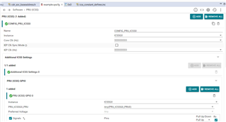
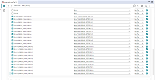
    You might be missing input enable configuration for pad, which can be done from Sysconfig itself


    After this you should be able to read input status from R31 register of PRU.

    I am able to evaluate this on my setup, please let us know if this issue persists.

    Thanks & Regards,
    Manoj.

  • Yes, that was the last missing piece. Just got back and was able to confirm reading input status on R31 now, also confirmed ability to switch direction during run time.