Tool/software:
Hello! I'd like to inquire about the detailed PCB LAYOUT of the Crystal block in a Multi Layer (2 or more layers).
As far as I know, there are about three important points, as follows:
-
When using a Ground barrier structure to isolate the Crystal, it's preferable to connect the Ground behind the Ground pin of the AP's Crystal with a single Via.
-
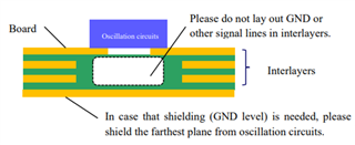
In a Multi-layer configuration, the bottom of the Crystal should be all Ground with no signal lines, and only the bottom layer should have a Ground Plane to shield against EMI.
-
The Ground path of External Capacitors should be kept as short as possible.

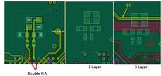
Now, let's consider the case mentioned above. Although it's a 6-layer PCB, for convenience, only 4 layers have been captured.
Question 1: Looking at the Top Layer, there is only one GND pin next to the XTAl pin, with a single via created next to it. In this case, wouldn't the Ground path of the Capacitor above the Top Layer become too long, causing an issue?
Question 2: The 2-layer setup has a clean Ground Plane. Doesn't this mean that ultimately there's no point in isolating on the Top layer? Shouldn't the isolation be the same for both layers? Like this:


Let me show you one more example. Although the diagram shows a 10-layer structure, only the layout of 4 layers has been brought.
Question 3: Why wasn't Ground isolated in this case? When is it better not to isolate?
Question 4: In the 3-layer setup, some signals including I2C Clk are passing through. Although they are not high-speed signals, does it matter since there is a Ground plane on the 2nd layer?
I apologize for the lengthy text, but the core of what I want to know is as follows:
Common Question 1: When grounding isolation, what is the most ideal number and placement of vias?
Common Question 2: When grounding isolation, is it better to eliminate even the Ground Plane on the 2nd layer or other inner layers?
Common Question 3: If there are power or signal lines on the 3rd layer and Ground plane must be placed on the 2nd layer, should this plane also be isolated?
I would greatly appreciate detailed explanations. There is no proper explanation in any of TI's Crystal PCB layout Guides.

