This thread has been locked.

If you have a related question, please click the "Ask a related question" button in the top right corner. The newly created question will be automatically linked to this question.

TDA4AL-Q1: RGMII Packet loss problem & clock

Part Number: TDA4AL-Q1

Tool/software:

Hello, sir

I implmented RGMII using TDA4AL and PHY (Realtek).

There are a total of 2 channels of RGMII on the board. One channel (main) does not experience packet loss at all, and the other channel (for debugging) experiences packet loss of up to 1%(already tried adjusting the delay.)

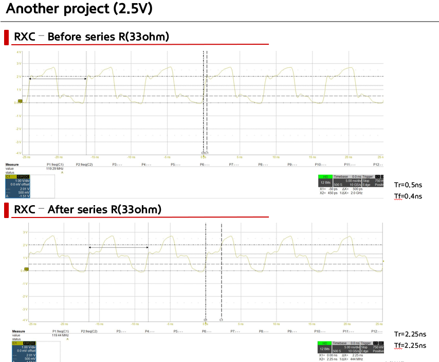
Actually, the TXC and RXC waveforms for both channels are not ideal,but there is no significant difference between two products.

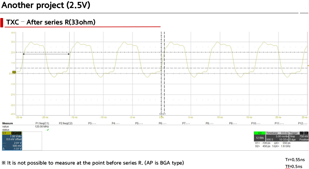
+ Another board using the same PHY (AP from another company) has similar waveforms but no packet loss.

1.  TXC does not reach the 3.3V level.(RXC reaches up to 3.3V.)  why??

 - The drive strength has already been adjusted. 

 - Any other option I can adjust?(ex. drive strength, impedance, termination...) 

   ※ It is unclear whether the cause of packet loss is the CLK waveform

2. If packet loss occurs, what are the ways the AP can adjust it?

- The length of the RGMII signal line is not that long, the length is matched, and solid GND planes are placed on the adjacent upper and lower layers.

- I 've never experienced a problem like this in any project using the same PHY that cannot be solved by adjusting the TXC and RXC delays.

1. chnnel2 - Main : no packet loss
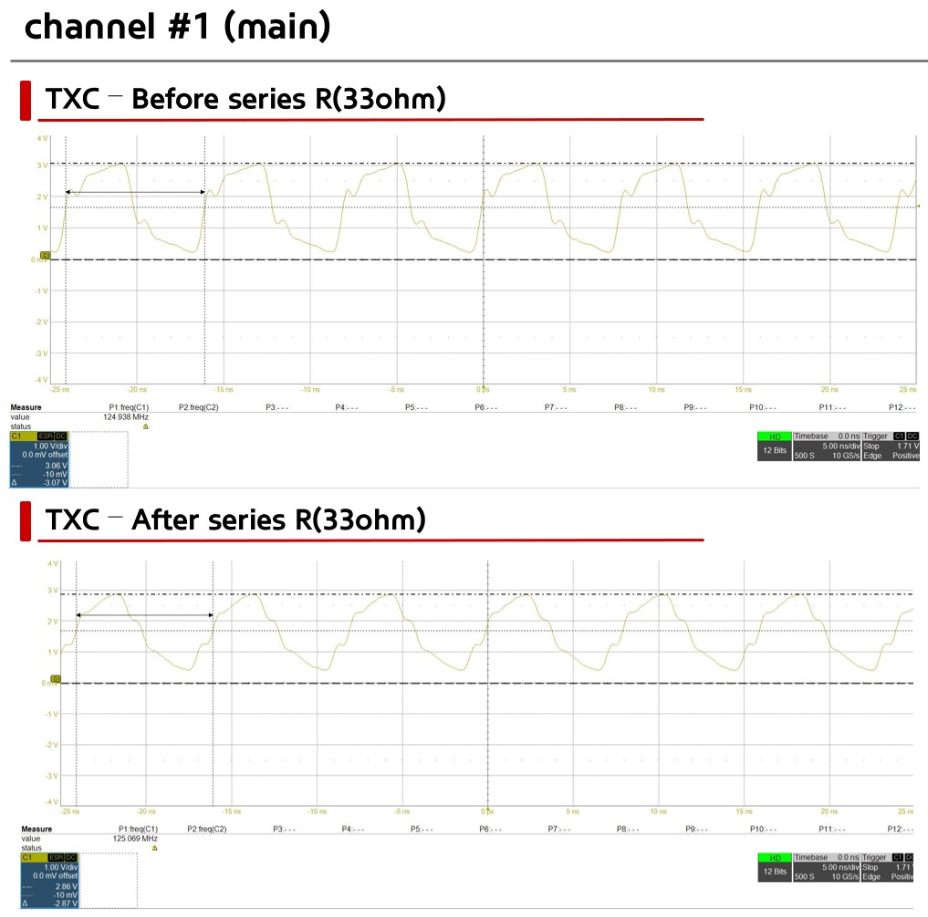
2. chnnel2 - for Debugging  : packet loss < 1%

3. Another project board (same PHY, different AP) - no packet loss
  • Hi,

    Which CPSW controls which RGMII? Is the debugging RGMII connected over MCU_CPSW2G?

    Which ethernet controllers control the RGMII links? ls it linux or ethfw or enet lld or mcal autosar driver.

    Can you provide the values of the following registers?

    • 0x40F04040
    • 0x00104034

    Regards,
    Tanmay

  • * CPSW

    RGMII(Main) - CPSW2G0

    RGMii(for debugging) - MCU_CPSW2G0 

    * Driver

    Using cpsw driver based on QNX (io-sock)

    * Register

    0x40F0_4040

    MCU_CTRL_MMR0_CFG0_CFG0_MCU_ENET_CTRL : 00000002(HEX)

    0x0010_4034

    CTRL_MMR0_CFG0_CFG0_CPSW2_ENET1_CTRL : 00000002 (HEX)

  • Hi,

    Can you just confirm that the same phy driver is being used for both the phys. What I was checking was the delay for the RGMII signal. From your question, it seems you have tried experimenting with the delay settings. From CPSW side, for both the RGMII connections, Tx delay is enabled from the MAC and Rx delay is supposed to be taken care of from the phy. You Can disable to TX delay from MAC side if you desire. Are you aware of the method to do so from QNX?

    What are the delay configuration set on the phy side? can you cross check it once.

    Was the schematic verified by TI? If not, is it possible for you share the schematic?

    Regards,
    Tanmay

  • Hi,


    - We are unsing the same driver(QNX io-sock) for the both the phys.


    - Currently, QNX knows where to set the delay and how to set the delay.
    In the default SDK code, it was recognized that the mask was not activated. so we set the Tx delay in AP.
    The datasheet below states "This internal delay is always enabled." It is written as, but when we checked, it was not enabled, so we enabled it.

    psdkqa\qnx\devnp\src\enetlld_if_utils.c >>
    EnetIfBoard_cpsw2gMacModeConfig function
    if (RGMII == mode)
    {
    regData |= (RGMII_ID_DISABLE_MASK); // We changed this line to a comment.
    }


    - Rx delay value set on PHY side
    # MAIN
    dev.rt9010phy.0.rxdly="1" // 1ns
    dev.rt9010phy.0.txdly="0"
    dev.rt9010phy.0.nossc="0"
    dev.rt9010phy.0.isr="2" //3.3v

    # DEBUG
    dev.rt9010phy.1.rxdly="1" //1ns
    #dev.rt9010phy.1.txdly="3" #befor AP delay
    dev.rt9010phy.1.txdly="1" //1ns #after AP delay
    dev.rt9010phy.1.nossc="1"
    dev.rt9010phy.1.isr="2"

    - Tx delay value set on PHY side
    When TX delay is enabled as specified in the data sheet, Tx seems to be delayed by 1.2ns.

    - The schematic was reviewed by TI.

  • Hi,

    Thanks for the confirmation and sorry for the delay.

    # DEBUG
    dev.rt9010phy.1.rxdly="1" //1ns
    #dev.rt9010phy.1.txdly="3" #befor AP delay
    dev.rt9010phy.1.txdly="1" //1ns #after AP delay
    dev.rt9010phy.1.nossc="1"
    dev.rt9010phy.1.isr="2"

    On the debug port, why is the phy txdelay 1ns after you added the delay in AP? can you make this 0, similar to what is being done for MAIN port.

    Have you confirmed that the delay is affecting the drops. Can you dump the stats and check the reason for the drops?

    The schematic was reviewed by TI.

    Was there an e2e for this? or was this done over a mail chain?

    Regards,
    Tanmay

  • By changing the delay settings, we found the delay value with the lowest loss during the ping test.

    We've tested the case below.

    No

    Test Case

    Register configuration for RX delay

    Register configuration for TX delay


    1

    TXC: no delay
    RXC: no delay

    1. Write Addr: 0x1B Data: 0xD04A
    2. Write Addr: 0x1C Data: 0x3

    1. Write Addr: 0x1B Data: 0xD084
    2. Write Addr: 0x1C Data: 0xC080


    2

    TXC: no delay
    RXC: 2ns delay

    1. Write Addr: 0x1B Data: 0xD04A
    2. Write Addr: 0x1C Data: 0x7

    1. Write Addr: 0x1B Data: 0xD084
    2. Write Addr: 0x1C Data: 0xC080


    3

    TXC: 1ns delay
    RXC: no delay

    1. Write Addr: 0x1B Data: 0xD04A
    2. Write Addr: 0x1C Data: 0x3

    1. Write Addr: 0x1B Data: 0xD084
    2. Write Addr: 0x1C Data: 0xC000
    3. Write Addr: 0x1B Data: 0xD084
    4. Write Addr: 0x1C Data: 0x0
    5. Write Addr: 0x1B Data: 0xD084
    6. Write Addr: 0x1C Data: 0x7


    4

    TXC: 1ns delay
    RXC: 2ns delay

    1. Write Addr: 0x1B Data: 0xD04A
    2. Write Addr: 0x1C Data: 0x7

    1. Write Addr: 0x1B Data: 0xD084
    2. Write Addr: 0x1C Data: 0xC000
    3. Write Addr: 0x1B Data: 0xD084
    4. Write Addr: 0x1C Data: 0x0
    5. Write Addr: 0x1B Data: 0xD084
    6. Write Addr: 0x1C Data: 0x7


    5

    TXC: 2ns delay
    RXC: no delay

    1. Write Addr: 0x1B Data: 0xD04A
    2. Write Addr: 0x1C Data: 0x3

    1. Write Addr: 0x1B Data: 0xD084
    2. Write Addr: 0x1C Data: 0xC000
    3. Write Addr: 0x1B Data: 0xD084
    4. Write Addr: 0x1C Data: 0x4000
    5. Write Addr: 0x1B Data: 0xD084
    6. Write Addr: 0x1C Data: 0x4007


    6

    TXC: 2ns delay
    RXC: 2ns delay

    1. Write Addr: 0x1B Data: 0xD04A
    2. Write Addr: 0x1C Data: 0x7

    1. Write Addr: 0x1B Data: 0xD084
    2. Write Addr: 0x1C Data: 0xC000
    3. Write Addr: 0x1B Data: 0xD084
    4. Write Addr: 0x1C Data: 0x4000
    5. Write Addr: 0x1B Data: 0xD084
    6. Write Addr: 0x1C Data: 0x4007


    7

    TXC: 3ns delay
    RXC: no delay

    1. Write Addr: 0x1B Data: 0xD04A
    2. Write Addr: 0x1C Data: 0x3

    1. Write Addr: 0x1B Data: 0xD084
    2. Write Addr: 0x1C Data: 0xC000
    3. Write Addr: 0x1B Data: 0xD084
    4. Write Addr: 0x1C Data: 0x8000
    5. Write Addr: 0x1B Data: 0xD084
    6. Write Addr: 0x1C Data: 0x8007


    8

    TXC: 3ns delay
    RXC: 2ns delay

    1. Write Addr: 0x1B Data: 0xD04A
    2. Write Addr: 0x1C Data: 0x7

    1. Write Addr: 0x1B Data: 0xD084
    2. Write Addr: 0x1C Data: 0xC000
    3. Write Addr: 0x1B Data: 0xD084
    4. Write Addr: 0x1C Data: 0x8000
    5. Write Addr: 0x1B Data: 0xD084
    6. Write Addr: 0x1C Data: 0x8007


    The data sheet says that internal delay is always enabled, but it was disabled in the code, so we enabled it.

  • Hi,

    Sorry for the delay.

    Allow me few days to follow-up on this.

    Regards,
    Tanmay