This thread has been locked.

If you have a related question, please click the "Ask a related question" button in the top right corner. The newly created question will be automatically linked to this question.

AM6442: DDR4 initialization failure with two-device (2 x 8-bit) DDR configuration of a custom board

Part Number: AM6442

Tool/software:

Hi TI experts,

I'm having trouble debugging the DDR4 initialization on my AM6442 custom board, which is a whole new design and does not boot up successfully, yet.

Could you provide some guidance to help me to solve this issue? Thanks.

Here are the details for your reference.

- SDK version: ti-processor-sdk-linux-am64xx-evm-09.02.01.09

  • "read DBI" is DISABLED manually (reference)

- Chip model: AM6442BSEFHAALV 34PL1JLS 709 G1 (HS-FS device, SR2.0)

- DDR4 chip: 

  • ISSI, IS43QR81024A-075VBLI K103
  • 1Gb x 8 bits x 2 devices = 2GB
  • not support "read DBI" function
  • datasheet is here: IS43QR81024A-075VBLI.pdf

- DDR4 DTSI

  • We keep most of the default setting from "DDR Register Configuration Tool in SysConfig," but make only 3 changes to the following parameters.
    1. Reference Design: TMDS64GPEVM
    2. Data Bus Width (per device): 8
    3. Density (per device) (Gb): 8

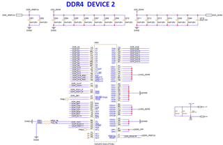
- Schematic (DDR interface from processor to memory)

  • This is the current status. Please for your information.

    Kind Regards,

    JDA.

  • Have you checked all the timing parameters from the DDR4 datasheet match the values in the tool?  The defaults values for the EVM in the tool is for a Micron device.  You need to go thru each parameter in case the ISSI datasheet has different values for each timing parameter.

    Regards,

    James

  • Hi James,

    I have checked all the timing parameters from ISSI DDR4 datasheet as you recommended and changed all the different parameters. But after testing, I still cannot get the DDR4 on my custom board to work properly.

    The following are the parameters I configured and the DDR chip model for your reference.

    1. DDR4 chip: 

    • ISSI, IS43QR81024A-075VBLI K103
    • 1Gb x 8 bits x 2 devices = 2GB
    • Page Size = 1KB
    • not support "read DBI" function
    • datasheet is here: IS43QR81024A-075VBLI.pdf

    2. The timing parameters and other setting are as follows.

    TI Default Online Setting New Setting via ISSI datasheet Note
    1. General Setting
    DDR Memory Type DDR4 DDR4
    Reference Design TMDS64GPEVM TMDS64GPEVM
    2. DDR4
    2.1 Config A) System Configuration
    Memory Frequency (MHz) 800 800
    Data Bus Width (per device) 16 8
    Density (per device) (Gb) 16 8
    Chip Selects / Ranks 1 1
    Operating Temperature Range -40C to 85C -40C to 85C
    Read DBI Enable Disable

    [P29][P274] "read DBI" is DISABLED manually (reference), due to this chip doesn't support it.

    LPASR mode Manual mode, Normal temp Manual mode, Normal temp
    TCR mode Disabled Disabled
    TCR range Normal Normal
    2.2 DRAM Timing A) Latency Parameters
    CL (nCK) 14 11 [P227] CAS Latency (not shown clearly)
    CWL (nCK) 9 9 [P129] CAS Write Latency (not sure 9 or 11?)
    primary choice = 9, alternative choice = 11
    CA Parity Latency 4 clocks 4 clocks [P29][P73]
    2.3 DRAM Timing B) Timing Parameters
    tCCD_L (tCK) 4 5 [P254] min = max(5nCK, 6.250ns)
    tCCD_L (ns) 5 6.25 [P254] min = max(5nCK, 6.250ns)
    tCCD_S (tCK) 4 4 [P255]
    tCKE (tCK) 3 3 [P66]
    tCKE (ns) 5 5 [P66]
    tCKSRE (tCK) 5 5 [P257]
    tCKSRE (ns) 10 10 [P257]
    tCKSRX (tCK) 5 5 [P257]
    tCKSRX (ns) 10 10 [P257]
    tDLLK (tCK) 597 597 [P255]
    tDQSCK min (ns) 0.16 0.225 [P256] -0.225 ns
    [reference][JDD] For DQSCKmin, keep the value of .225.  This is taken as a negative value.
    tDQSCK max (ns) 0.16 0.225 [P256] -0.225 ns
    [reference][JDD] For DQSCKmin, keep the value of .225.  This is taken as a negative value.
    tFAW (tCK) 28 20 [P255] page size of this chip is 1KB
    tFAW_1K, Min=Max(20nCK, 25ns)
    tFAW_2K, Min=Max(28nCK, 35ns)
    tFAW (ns) 30 25 [P255] page size of this chip is 1KB
    tFAW_1K, Min=Max(20nCK, 25ns)
    tFAW_2K, Min=Max(28nCK, 35ns)
    tMOD (tCK) 24 24 [P255]
    tMOD (ns) 15 15 [P255]
    tMRD (tCK) 8 8 [P255]
    ODTH8 (tCK) 6 6 [P191] not sure 6 or 7?
    1 tCK Preamble = 6, 2 tCK Preamble = 7
    tPAR_ALERT_PW max (tCK) 192 96 [P258] Min=48, Max = 96
    (The max value is inputted here.)
    tPW_RESET_L (ns) 200000 200000 [P204]
    2.3 DRAM Timing B) Timing Parameters
    tRAS (ns) 35 35 not shown for DDR4-1600, use the default
    tRCD (ns) 13.75 13.75 not shown for DDR4-1600, use the default
    tREFI (ns) 7800 7800 [P101] 1X mode, 8Gb , tREFI1 = 7.8us
    tRFC (ns) 350 350 [P101] 1X mode, 8GB, tRFC1(min) = 350 ns
    tRP: (ns) 13.75 13.75 not shown for DDR4-1600, use the default
    tRRD_L (tCK) 4 4 [P255] page size of this chip is 1KB
    tRRD_L(1K), Min = Max(4nCK, 6ns)
    tRRD_L(2K), Min = Max(4nCK, 7.5ns)
    tRRD_L (ns) 6.4 6 [P255] page size of this chip is 1KB
    tRRD_L(1K), Min = Max(4nCK, 6ns)
    tRRD_L(2K), Min = Max(4nCK, 7.5ns)
    tRRD_S (tCK) 4 4 [P255] page size of this chip is 1KB
    tRRD_S(1K),Min=Max(4nCK,5ns)
    tRRD_S(2K),Min=Max(4nCK,6ns)
    tRRD_S (ns) 5.3 5 [P255] page size of this chip is 1KB
    tRRD_S(1K),Min=Max(4nCK,5ns)
    tRRD_S(2K),Min=Max(4nCK,6ns)
    tRTP (tCK) 4 4 [P255]
    tRTP (ns) 7.5 7.5 [P255]
    tWR (ns) 15 15 [P255]
    tWR_CRC_DM (tCK) 4 4 [P255]
    tWR_CRC_DM (ns) 3.75 3.75 [P255]
    tWTR_L (tCK) 4 4 [P255]
    tWTR_L (ns) 7.5 7.5 [P255]
    tWTR_S (tCK) 2 2 [P255]
    tWTR_S (ns) 2.5 2.5 [P255]
    tWTR_S_CRC_DM (tCK) 4 4 [P255]
    tWTR_S_CRC_DM (ns) 3.75 3.75 [P255]
    tXP (tCK) 4 4 [P257]
    tXP (ns) 6 6 [P257]
    tXPR (tCK) 5 5 [P257]
    2.4 IO Control A) Processor / DDR Controller IO Configuration
    VREF Control Range DQ/DM Range 1 Range 1 not sure, yet, use the default
    VREF Control % of VDDQ DQ/DM 72.8 72.8 not sure, yet, use the default
    Driver Impedance for DQ/DQS/DM 40 Ohm 40 Ohm not sure, yet, use the default
    Driver Impedance for Addr/Ctrl/Clk 40 Ohm 40 Ohm not sure, yet, use the default
    ODT for DQ/DQS/DM 48 Ohm 48 Ohm not sure, yet, use the default
    2.5 IO Control B) DRAM IO Configuration
    DQ VREF Range Range 1 Range 1 not sure, yet, use the default
    DQ VREF 72.4 72.4 not sure, yet, use the default
    Output Driver Impedance (ODI) RZQ/7(34ohm) RZQ/7(34ohm) not sure, yet, use the default
    Nominal ODT (RttNOM) RZQ/6(40ohm) RZQ/6(40ohm) not sure, yet, use the default
    Dynamic ODT Disabled Disabled not sure, yet, use the default

    After using the new setting, the AM6442 boot process still fails as before.

    I am not sure if the DDR4 configuration is correct or not. Or there are still something else we need to check again?

    Please provide further guidance or indication, if you may.

    Figure 1: The boot log of the new DDR4 configuration (20240608-1420).

    Kind Regards,

    JDA.

  • Hi JDA,

    the changes you made to the configuration look correct.

    One thing i noticed on the schematic is that DDR_RESETn should be pulled low thru a resistor (see page 9 of the DDR datasheet).  This signal should be low during power ramp, and the pull resistor low will ensure this.  I'm not sure if this is the main problem, but please try to correct this on one of your boards.

    Check RESET vs CKE on a scope.  CKE should go high at least 500ns after RESET goes high.  This ensures the initialization starts correctly.

    Can you send the .dtsi file that you are using?

    Regards,

    James

  • Hi James,

    Thanks for reviewing the DDR4 configurations for us.

    The .dtsi file which I am using and generated from “TI DDR Register Configuration Tool in SysConfig” service is attached as a .zip file below. 

    The source code of "k3-am64-evm-ddr4-1600MTs.dtsi" is replaced with the content of this .dtsi file.

    Meanwhile, the "k3-am64-ddr.dtsi" and other related .dtsi files are kept as the original without any modification.

    (SDK version: ti-processor-sdk-linux-am64xx-evm-09.02.01.09)

    PS: We also appreciate for your kind reminder and guidance for "DDR_RESETn" issue. We are trying to fix it now. For any further update or good news, I will let you know.

    Kind Regards,

    JDA.

    [download] k3-am64-ddr-config_disable-readDBI.zip

  • I noticed a few changes that need to be made to the configuration.  Since you are using a -075 device, you have to look at the DDR4-2666 speed bin table (pg 227) for some of the parameters.

    For 800MHz (1.25ns) only CL=12 is valid, other choices are reserved.  There are 2 choices for CWL, i would stay with 9

    tRP = 14.25ns

    tRCD=14.25ns

    Please make these changes and send the .dtsi file again.

    Also, can you also try to apply the attached patch?  This will add code that will dump the DDR subsystem registers to the console.  Please copy that to a file and post here.  This will give me some visibility into the training results.

    To apply patch, cd to the u-boot directory and run:

    git apply 0001-added-regdump-code.patch

    The patch include 2 new files, and some minor edits to the DDR driver to call the regdump code

    /cfs-file/__key/communityserver-discussions-components-files/791/0001_2D00_added_2D00_regdump_2D00_code.patch

    Regards,

    James

  • Hi James,

    We've followed your guidance to modify our schematic. Now, the DDR_RESETn is pulled low through a resistor. 

    After checking the DDR_RESETn vs DDR_CKE signal on a scope, the sequence seems not to be as expected. (page 9,10 of DDR datasheet)

    CKE goes to be HIGH firstly. After about 2.5 seconds, DDR_RESETn goes to be HIGH then.

    Do you have any idea about the possible reason of this unexpected result? Is it because of the DDR configuration of .dtsi? 

    PS: The .dtsi file tested here is the previous version without changing CL=12, yet. But we will implement your kind guidance and try to dump the DDRSS registers to the console in the coming 24 hours. Appreciates.
    [download] k3-am64-ddr-config_disable-readDBI.zip


    (page 10 of DDR datasheet)

    (page 9 of DDR datasheet)

    Kind Regards,

    JDA.

  • Yes, the relationship between CKE and RESET is not correct.  But i'm trying to understand the scale you have setup on your scope.  RESET should rise to 1.2V, but i only see it go to less than 500mV.  CKE is VTT terminated, so its level is ok (although i can't explain the slight glitch before it goes high).

    Please double check the rework on RESET signal.  And take a wider scope shot, you should see RESET low during power ramp, and then transition to 1.2V once and stay high

    Regards,

    James

  • Hi James,

    By following your kind advice, the four DDR4 parameters are updated into our .dtsi file, which is attached as below. Meanwhile, the .patch file you provided is merged into our source code. The DDR subsystem registers now are able to be dumped to the console. The console log is also attached as below for your reference. Thanks.

    • CL = 12
    • CWL = 9
    • tRP = 14.25 ns
    • tRCD = 14.25 ns

    PS: There is no hardware modification for above firmware test, yet. But we appreciate your kind reminder of the CKE/RESET issue. We are working on it now.

    k3-am64-ddr-config_disable-readDBI_CL-12_v20240614-2247.zip

    [20240613-2247] Dump_DDRSS_Registers.log
    Fullscreen
    1
    2
    3
    4
    5
    6
    7
    8
    9
    10
    11
    12
    13
    14
    15
    16
    17
    18
    19
    U-Boot SPL 2023.04 (Jun 13 2024 - 22:47:27 +0800)
    Resetting on cold boot to workaround ErrataID:i2331
    Please resend tiboot3.bin in case of UART/DFU boot
    resetting ...
    U-Boot SPL 2023.04 (Jun 13 2024 - 22:47:27 +0800)
    SYSFW ABI: 3.1 (firmware rev 0x0009 '9.2.7--v09.02.07 (Kool Koala)')
    k3_ddrss_probe(dev=)
    k3_ddrss_ofdata_to_priv(dev=)
    k3_ddrss memorycontroller@f300000: ddr freq0 not populated, using bypass frequency.
    k3_ddrss_power_on(ddrss=)
    k3_ddrss memorycontroller@f300000: VTT regulator enabled, volt = 0
    k3_lpddr4_probe: PASS
    k3_lpddr4_init: PASS
    --->>> LPDDR4 Initialization is in progress ... <<<---
    k3_lpddr4_start: Post start PASS
    Begin DDR Register Dump
    0x0f308000 0x10460a01 //DDRSS_CTL_0_DATA
    0x0f308004 0x5d1af3c3 //DDRSS_CTL_1_DATA
    XXXXXXXXXXXXXXXXXXXXXXXXXXXXXXXXXXXXXXXXXXXXXXXXXX

    Kind Regards,

    JDA.

  • The regdumps are showing that the training isn't working at all, most likely indicating that something is wrong early on.  Certainly the CKE/RESET relationship is wrong, but that may be caused by something else, since that is a very fixed part of the hardware sequencing.  Please check the basics:

    -ensure all DDR voltage rails are at the correct level and stable before RESET  and CKE go high:

    Processor voltage rails:

    VDDS_DDR = VDDS_DDR_C = 1.2V

    VDDA_PLL1 = 1.8V

    VDD_CORE = 0.75 or 0.85V

    Memory voltage rails:

    VTT = 0.6V

    DDR_VREFCA = 0.6V

    DDR_VPP = 2.5V

    you can check others, but these are the main ones associated with the DDR.

    -probe DDR_CK to see if it is 800MHz

    Regards,

    James

  • Hi James,

    By following your kind advice, we've fixed some hardware issues and ensured each voltage rails are at correct levels as you reminded, respectively.

    You may check their status as below. Meanwhile, the new log content is also attached here.

    • If it is possible, could you review the new log for us?

    • Does the log mean our DDR initialization come to ready and work well? Which log message is your key identifier?

    • In addition, the boot process stops at the following point. Could you provide us further guidance, if you may? (Which stages has our boot process passed? At which stage our boot process currently stuck? Is it possible to do the memory test at current status?)
      • [   12.014182] platform fixed-regulator-sd: deferred probe pending

    PS: Thanks for being with us with patience as we improve our AM6442 custom board, recently.

    Fullscreen
    1
    2
    3
    4
    5
    6
    7
    8
    9
    10
    11
    12
    13
    14
    15
    16
    17
    18
    19
    20
    21
    U-Boot SPL 2023.04 (Jun 14 2024 - 07:59:55 +0800)
    Resetting on cold boot to workaround ErrataID:i2331
    Please resend tiboot3.bin in case of UART/DFU boot
    resetting ...
    U-Boot SPL 2023.04 (Jun 14 2024 - 07:59:55 +0800)
    SYSFW ABI: 3.1 (firmware rev 0x0009 '9.2.7--v09.02.07 (Kool Koala)')
    k3_ddrss_probe(dev=)
    k3_ddrss_ofdata_to_priv(dev=)
    k3_ddrss memorycontroller@f300000: ddr freq0 not populated, using bypass frequency.
    k3_ddrss_power_on(ddrss=)
    k3_ddrss memorycontroller@f300000: VTT regulator enabled, volt = 0
    k3_lpddr4_probe: PASS
    k3_lpddr4_init: PASS
    --->>> LPDDR4 Initialization is in progress ... <<<---
    k3_lpddr4_start: Post start PASS
    Begin DDR Register Dump
    0x0f308000 0x10460a01 //DDRSS_CTL_0_DATA
    0x0f308004 0x5d1af3c3 //DDRSS_CTL_1_DATA
    0x0f308008 0x0171a610 //DDRSS_CTL_2_DATA
    0x0f30800c 0x40020a11 //DDRSS_CTL_3_DATA
    XXXXXXXXXXXXXXXXXXXXXXXXXXXXXXXXXXXXXXXXXXXXXXXXXX

    Kind Regards,

    JDA.

  • HI JDA,

    yes, the log looks much better now, looks like training is completing successfully and the boot is proceeding.  There is not really an indicator of successful DDR training, but the fact that the boot continues past this line:

    SPL initial stack usage: 13408 bytes

    Indicates that the DDR is working.  You will probably need to perform memory stress tests across temperature to further test the robustness of the DDR configuration.

    You can now revert the patch as you don't need the debug messages and the DDR regdump anymore.

    It looks like now the boot is failing to read the device tree file, or there is something wrong with the DTB.  I will have to pass the thread off to another colleague to help with that.

    Regards,

    James

  • Hi JDA,

    [    1.909414] mmc0: SDHCI controller on fa10000.mmc [fa10000.mmc] using ADMA 64-bit
    [    1.917210] Waiting for root device PARTUUID=6dd013bc-02...
    [   11.998550] platform mdio-mux-1: deferred probe pending
    [   12.003852] platform leds: deferred probe pending
    [   12.008600] platform mux-controller: deferred probe pending
    [   12.014182] platform fixed-regulator-sd: deferred probe pending

    It appears your board boots from SD card, but the end of the kernel boot log shows the SD card is not detected (mmc1 on fa000000.mmc). And the issue seems to be in the SD card I/O voltage switching. (The U-Boot boot log already shows voltage switching failed.)

    Please check your kernel device tree "fixed-regulator-sd" node and its related settings, likely the switch is controlled by a GPIO. Please review all this information and ensure it matches your board design.

  • Hi Bin,

    Because the SD Card circuit of our customized board only supports the 3.3V power supply and does not yet support the 1.8V power circuit, yet.

    Could this be the reason for the boot failure when switching from 3.3V to 1.8V, thus causing the SD Card incapable of being read?

    If so, how can I set the device tree to fix the SD Card (mmc1) voltage at 3.3V only and prevent it from switching to 1.8V mode?

    Please assist me with this, if you may. 


    PS: Thanks for your kind guidance.

    Here is my current fixed-regulator-sd node description of kernel device tree, which comes from the original file of k3-am642-evm.dts. 

    Fullscreen
    1
    2
    3
    4
    5
    6
    7
    8
    9
    10
    11
    vdd_mmc1: fixed-regulator-sd {
    /* TPS2051BD */
    compatible = "regulator-fixed";
    regulator-name = "vdd_mmc1";
    regulator-min-microvolt = <3300000>;
    regulator-max-microvolt = <3300000>;
    regulator-boot-on;
    enable-active-high;
    vin-supply = <&vsys_3v3>;
    gpio = <&exp1 6 GPIO_ACTIVE_HIGH>;
    };
    XXXXXXXXXXXXXXXXXXXXXXXXXXXXXXXXXXXXXXXXXXXXXXXXXX

    Kind Regards,

    JDA.

  • Hi JDA,

    To prevent SD card to switch to 1.8v, please add the following property to the &MMC1 node in your board device tree.

    no-1-8-v;

  • Hi Bin,

    By following your guidance, here we've added "no-1-8-v;" to the k3-am642-evm.dts file of the following location.

    But the situation is still the same, is there anything we are missing? Please guide us if you may.

    • DTS file:
      /opt/ti-processor-sdk-linux-am64xx-evm-09.02.01.09/board-support/u-boot-build/a53/source/arch/arm/dts/k3-am642-evm.dts

    Fullscreen
    1
    2
    3
    4
    5
    6
    7
    8
    &sdhci1 {
    /* SD/MMC */
    vmmc-supply = <&vdd_mmc1>;
    pinctrl-names = "default";
    pinctrl-0 = <&main_mmc1_pins_default>;
    disable-wp;
    no-1-8-v; /* disabling all the UHS modes, added by JDA */
    };
    XXXXXXXXXXXXXXXXXXXXXXXXXXXXXXXXXXXXXXXXXXXXXXXXXX

    Kind Regards,

    JDA.

  • Hi JDA,

    DTS file:
    /opt/ti-processor-sdk-linux-am64xx-evm-09.02.01.09/board-support/u-boot-build/a53/source/arch/arm/dts/k3-am642-evm.dts

    I was asking to add "no-1-8-v;" to kernel board device tree, not U-Boot.

    BTY, kernel provides two board dts for the two AM64x EVM: k3-am642-evm.dts and k3-am642-sk.dts. Please ensure you modify the one used for your board.