Because of the Thanksgiving holiday in the U.S., TI E2E™ design support forum responses may be delayed from November 25 through December 2. Thank you for your patience.

This thread has been locked.

If you have a related question, please click the "Ask a related question" button in the top right corner. The newly created question will be automatically linked to this question.

[FAQ] TMUX1308-Q1: EN and Control inputs termination - AM62P, AM62A use case

Part Number: TMUX1308-Q1
Other Parts Discussed in Thread: TMUX1308, AM625, TMUX1308A, SN74LV4051A, TMUX1308A-Q1, ADC121S101, , TPS65224-Q1

Tool/software:

Hi Team,

TMUX1308 EN and control A0..A2 is being controlled by AM625 Sitara SOC.

SOC IO buffers are off during power-up. The IOs are in high impedance and expected to take 1..2 seconds to be initialized to a known state.

Do you have any recommendation of connecting the EN and the control inputs during this period. 

Are the TMUX EN and address control inputs A0..2 tolerant to being open for some time ( 1..2 sec)  during power cycle until the SOC IOs are initialized.

Thank you for the support.

Regards,

Sreenivasa

  • Hey Sreenivasa,

    Am I understanding properly that the supply will ramp up first then the I/O's (Sx/D) will take a second or 2 to turn on? 
    While the I/O's have some time to initialize to a known state, do we have the same restrictions on the control pin. Ideally I would tie the EN pin high to isolate the inputs/outputs of the device until the signals are ready.

    Are the TMUX tolerant to the inputs being open for some time during power cycle.

    Which inputs are you referring to here?
    The control inputs (Ax) are tolerant and can take up to 5.5V regardless of the supply voltage. 
    Source and Drain inputs Sx and D are recommended to keep between GND and VDD but there are some protection features here that will allow you to exceed those values if you limit the current.

    Thanks,
    Rami

  • Hello Rami, 

    Thank you for the inputs.

    Are the TMUX EN and address control inputs A0..2 tolerant to being open for some time ( 1..2 sec)  during power cycle until the SOC IOs are initialized.

    I updated the question above,

    Am I understanding properly that the supply will ramp up first then the I/O's (Sx/D) will take a second or 2 to turn on? 
    While the I/O's have some time to initialize to a known state, do we have the same restrictions on the control pin. Ideally I would tie the EN pin high to isolate the inputs/outputs of the device until the signals are ready.

    The SOC IOs controlling the Ax/EN will be in High impedance expected to take 1..2 seconds to be initialized to a known state. The TMUX inputs would be floating during this time.

    Any thoughts please.

    Regards,

    Sreenivasa


  • Ah I understand now. So the control pins will be floating for a couple seconds. I'd recommend a weak pull up on the EN/ line. Just to hold the state while it's floating to disable all the channels. You can then pull it down when the the initialization period is complete.

    Thanks,
    Rami

  • Hello Rami, 

    Thank you for the inputs.

    Understand the recommendations.

    In case the /EN is permanently enabled by hard wiring, do you have some recommendations on connecting the A0..A2 if the SOC takes 1..2 seconds to configure the address.

    Regards,

    Sreenivasa

  • Hey Sreenivasa,

    You could try a weak pulldown but know that your S0 path would be turned on for that 1-2second configuration

    Thanks,
    Rami

  • Hello Rami, 

    Thank you.

    The TMUX output is typically connected to the ADC input.

    Would it be Ok to connect a 100 nF cap directly at the output of the MUX. If not is there a recommended value.

    The cap recommended on the supply ranges from 0.1 uF to 10 uF. Could you please guide on the recommended cap value and the rationale to choose the cap value.

    Regards,

    Sreenivasa

  • Hey Sreenivasa,

    Yes, you can add a 100nF cap directly on the output of the mux. What is the purpose of the cap though?

    The cap on the power supply is a decoupling cap that filters out noise on the power supply line. The values are selected so that higher frequency noise (kHz to MHz range) are filtered and your supply signal will be smooth.

    Thanks,
    Rami

  • Hello Rami, 

    Thank you.

    I do not have complete insight but looks like customer is measuring DC voltages and temperature inputs and might want to use the cap as the filter rather than RC.

    Any thoughts please.

    Regards,

    Sreenivasa

  • Hey Sreenivasa,

    No problems at all using the cap on the output of the mux as a filter!

    Thanks,
    Rami

  • Hello Rami, 

    Thank you.

    No problems at all using the cap on the output of the mux as a filter!

    I assume You do not see any concern connecting the cap directly to the MUX output.

    Thank you for the support.

    Regards,

    Sreenivasa

  • Hi Board designers, 

    Additional inputs on TMUX1308 vs TMUX1308A

    Customer is now evaluating TMUX1308 as a replacement of SN74LV4051A, and found a glitch on output (D) pin on TMUX1308 which cannot be seen with SN74LV4051A.

    Here is scope captures customer took for SN74LV4051A and TMUX1308.
    Ch1 (Yellow): A/A0 (pin 11)
    Ch2 (Cyan): INH/EN (pin 6)
    Ch3: (Purple): Yx/Sx
    Ch4: (Green): COM/D (pin 3)

    Customer just replaced SN74LV401A with TMUX1308 and no other change was applied. Also customer confirmed the same phenomenon with 4 TMUX1308 units.
    Customer is asking us;
    1. Why does the glitch (surrounded by blue rectangle) with synchronizing to pin 11 happens?
    2. Why TMUX1308's ramping slew rate (surrounded by red rectangle) is faster than SN74LV4051A?

    Regards,

    Sreenivasa

  • Hi Board designers, 

    Additional inputs on TMUX1308 vs TMUX1308A continued

    Thanks for reaching out. Can you share the schematic being used here? We have seen this phenomenon before where the TMUX1308 is being fed into an ADC. When channels are being toggled quickly, there is a settling time phenomenon exhibited by the TMUX1308 when there are large resistors are the input to the mux. These resistors can be sized down to alleviate the issue, but having the schematic to check would be helpful.

    Note that we have recently released the TMUX1308A-Q1 which is optimized for these situations so if you wish to sample those, the product is live on TI.com


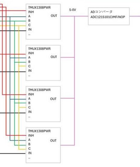
    Customer is connecting TMUX1308 output to our ADC121S101 as below. The scope capture is just focusing on single TMUX1308, and other output of TMUX1308 are in HiZ.


    Thanks for the info. My previous explanation still stands that this is a phenomenon exhibited by the TMUX1308 when placed in front of an ADC under certain conditions. As mentioned, you can try to size down the resistors as a first step. Since the device has injection current control feature/short to battery protection, the output will be clamped to VDD + VT as long as current through the switch is limited. A second step is to get samples of the TMUX1308A which is optimized for these conditions and see if that fixes the issue as well.


    I understand the injection current control will limit current on the switches, but still wonder why this phenomenon is seen when the output is fed by ADC? The glitch is happening at the timing of changing TMUX1308 source. It is not synchronizing with ADC's behavior, such as S/H cap charging. Could you please explain why?


    This phenomenon is related to the injection current control feature of the device and not being optimized for high impedance loads such as an ADC. The device does not have sufficient built in delay on the internal pulldown switch when it toggles on/off. So, there is a discharging effect, therefore we see the drop on the signal path before it eventually settles back at the target voltage. This behavior was changed with the TMUX1308A - a delay was added to the internal pulldown switch, so it won’t dump all the current and cause the signal to dip. So I strongly urge the customer to sample the TMUX1308A as it's likely to solve the issue seen here.

    Regards,

    Sreenivasa

  • Hi Board designers, 

    Inputs on TMUX1308 paralleling 

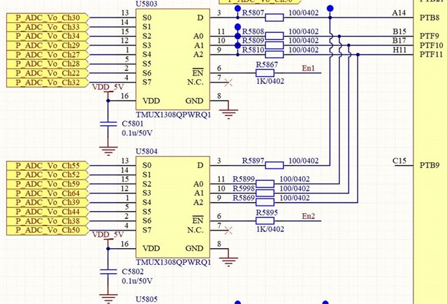
    Could our TMUX1308-Q1 be used in parallel as shown below?

    The customer's schematic is as follows, 2 TMUX1308s are used in parallel to achieve the effect of expanding 16, and the selected channels are distinguished through the ENx Pin and the address Pin.

    Will the disabled TMUX1308 interfere with another TMUX1308?

    In theory, can multiple TMUX1308s be used in parallel? For example, 2 pieces, 3 pieces, 4 pieces...

    The transmitted signal is analog signal, such as output voltage sampling, output current sampling.

    The switching frequency between each channel is about 500Hz.

    Regards,

    Sreenivasa

  • Hi Board designers, 

    Additional inputs on TMUX1308 paralleling 

    You certainly can run them in parallel like this. In theory, the limitations on how much you can use will vary from application to application. Every time you add a mux and short the drain together, you'll be adding the Drain Off Capacitance of the unselected to the On capacitance of the selected channel. So for 2 TMUX1308's you'll have 11pF On-capacitance plus 7pF Drain off Capacitance. Adding capacitance will decrease the bandwidth that the device can support. That being said, this is typically a 500MHz device so adding 7pF should very easily support the 500Hz need. 
    Another thing to take into consideration would be the leakage. Not only would on-leakage be present but also the drain off-leakage of the off channels that are shorted together. Leakage on this device is fairly low so I wouldn't be too worried with 2 devices but as you start increasing more and more devices in parallel, it's something to keep an eye out. More leakage will reduce the accuracy of the measurements.

    Regards,

    Sreenivasa

  • Hi Board designers,  

    TMUX1308 output level configuration

    When interfacing the  TMUX1308 to TPS65224-Q1, 

    https://www.ti.com/product/TPS65224-Q1

    The ADC_IN range of the PMIC is as below 

    From GPIO pin assigned as ADC_IN to ground. If GPIO4 is used as ADC_IN, VADC_IN ≤ VIO. If GPIO5 is used as ADC_IN, VADC_IN ≤ 1.8V

    Regards,

    Sreenivasa