This thread has been locked.

If you have a related question, please click the "Ask a related question" button in the top right corner. The newly created question will be automatically linked to this question.

TDA4VH-Q1: HFOSC1 oscillator should be used for the A72 (MAIN domain) and GTC

Part Number: TDA4VH-Q1

Tool/software:

Hello,

Due to a safety guideline, we want to use the HFOC1 oscillator for the A72 (MAIN DOMAIN) and the GTC TIMER.

Board: J784s4 custom board
PDK: 09.02.00.30
Linux
SPL Boot

To achieve it I have seen that following PLLs base clock oscillator have to be switched

PLL0 (MAIN PLL) -> MAIN_PLL0_HSDIV6_CLKOUT -> GTC Timer
PLL8 (ARM0 PLL - A72 cluster 0)
PLL9 (ARM1 PLL - A72 cluster 1)
PLL14(R5FSS PLL - R5F main domain)

Our current setup is, that at in the MCU 1_0 firmware the MAIN domain PLL's are initialized by the assistant of the sciclient  -> running at the default HFOSC0
Afterward the registers of the concerning PLLs are modified with:

-> enable HFSOC1 oscillator
-> disable PLL0, PLL8 and PLL9.
-> switch base oscillator to hfsoc1
-> adjust gain to get from 22579200Hz to 2GHZ
-> enable PLLs again and wait for LOCK.

Is this really a good approach or would it better to adjust the sciclient code to achieve the required behavior?
( "packages/ti/drv/sciclient/src/rm_pm_hal/pm/soc/j784s4/clocks.c")

Following routine, located at ("packages/ti/drv/sciclient/src/rm_pm_hal/pm/drivers/clock"), is responsible to setup the PLLs depending
of the hardware specific configuration located at j784s4/clocks.c
"const struct pll_table_entry soc_pll_table[91]

static u32 clk_pll_16fft_internal_set_freq_from_pll_table(struct clk *pll_clk,
							  struct clk *div_clk,
							  const struct pll_data *pll_data_t,
							  u32 target_hz,
							  u32 min_hz,
							  u32 max_hz,
							  sbool query, sbool *changed)


If yes do you have any patch or some tips what have to be done?

Kind Regards
Thomas Willetal

  • Hello,

    regarding to my question I have some additional information:

    The current frequency of the oscillators is:
    HFSOC0 (default) : 19200000Hz
    HFSOC1                 : 22579200Hz

    We wanted to keep the generated PLL frequencies to the same value as before the HFSOC1 switch over and so we adjusted only the GAIN.
    It is caused by the different oscillator frequency.

    The register values of the different PLLs after the HFSOC1 oscillator switch over are:


    HFOSC1 * (PLL0_FREQ_CTRL0 + PLL0_FREQ_CTRL1/2^24) = PLL_FREQ
    22579200Hz * ( 0x58(88) + 0x0093bcaa(9682090)/2^24) = 2000000001Hz
    
    --- MAIN PLL0 ------------------------------------
    PLL0_PID: 0x61801001
    PLL0_CFG: 0x01ff0801
    PLL0_LOCKKEY0: 0x68ef3491
    PLL0_LOCKKEY1: 0xd172bc5a
    PLL0_CTRL: 0x00018013
    PLL0_STAT: 0x00000001
    PLL0_FREQ_CTRL0: 0x00000058
    PLL0_FREQ_CTRL1: 0x0093bcaa
    PLL0_DIV_CTRL: 0x01020001
    PLL0_SS_CTRL: 0x80000000
    PLL0_SS_SPREAD: 0x00010001
    PLL0_CAL_CTRL: 0x00020000
    PLL0_CAL_STAT: 0x00000000
    PLL0_HSDIV0_CTRL0: 0x00008003
    PLL0_HSDIV1_CTRL0: 0x00008004
    PLL0_HSDIV2_CTRL0: 0x00008009
    PLL0_HSDIV3_CTRL0: 0x0000800e
    PLL0_HSDIV4_CTRL0: 0x00008018
    PLL0_HSDIV5_CTRL0: 0x00008013
    PLL0_HSDIV6_CTRL0: 0x00008004
    PLL0_HSDIV7_CTRL0: 0x00008004
    PLL0_HSDIV8_CTRL0: 0x00008003
    
    --- MAIN PLL8 ------------------------------------
    PLL8_PID: 0x61801001
    PLL8_CFG: 0x00010801
    PLL8_LOCKKEY0: 0x68ef3491
    PLL8_LOCKKEY1: 0xd172bc5a
    PLL8_CTRL: 0x00018013
    PLL8_STAT: 0x00000001
    PLL8_FREQ_CTRL0: 0x00000058
    PLL8_FREQ_CTRL1: 0x0093bcaa
    PLL8_DIV_CTRL: 0x01020001
    PLL8_SS_CTRL: 0x80000000
    PLL8_SS_SPREAD: 0x00010001
    PLL8_CAL_CTRL: 0x00020000
    PLL8_CAL_STAT: 0x00000000
    PLL8_HSDIV0_CTRL0: 0x00008000
    
    --- MAIN PLL9 ------------------------------------
    PLL9_PID: 0x61801001
    PLL9_CFG: 0x00010801
    PLL9_LOCKKEY0: 0x68ef3491
    PLL9_LOCKKEY1: 0xd172bc5a
    PLL9_CTRL: 0x00018013
    PLL9_STAT: 0x00000001
    PLL9_FREQ_CTRL0: 0x00000058
    PLL9_FREQ_CTRL1: 0x0093bcaa
    PLL9_DIV_CTRL: 0x01020001
    PLL9_SS_CTRL: 0x80000000
    PLL9_SS_SPREAD: 0x00010001
    PLL9_CAL_CTRL: 0x00120000
    PLL9_CAL_STAT: 0x00000000
    PLL9_HSDIV0_CTRL0: 0x00008000
    
    --- MAIN PLL14 ------------------------------------
    PLL14_PID: 0x61801001
    PLL14_CFG: 0x00070801
    PLL14_LOCKKEY0: 0x68ef3491
    PLL14_LOCKKEY1: 0xd172bc5a
    PLL14_CTRL: 0x00018013
    PLL14_STAT: 0x00000001
    PLL14_FREQ_CTRL0: 0x00000058
    PLL14_FREQ_CTRL1: 0x0093bcaa
    PLL14_DIV_CTRL: 0x01020001
    PLL14_SS_CTRL: 0x80000000
    PLL14_SS_SPREAD: 0x00010001
    PLL14_CAL_CTRL: 0x00120000
    PLL14_CAL_STAT: 0x00000000
    PLL14_HSDIV0_CTRL0: 0x00008001
    PLL14_HSDIV1_CTRL0: 0x00008001
    PLL14_HSDIV2_CTRL0: 0x00008001


    k3conf output:

    jolly-joliot ~ # k3conf dump processor
    |------------------------------------------------------------------------------|
    | VERSION INFO                                                                 |
    |------------------------------------------------------------------------------|
    | K3CONF | (version 0.3-nogit built Thu Feb 29 11:51:13 UTC 2024)              |
    | SoC    | J784S4 SR1.0                                                        |
    | SYSFW  | ABI: 3.1 (firmware version 0x0009 '9.2.4--v09.02.04 (Kool Koala))') |
    |------------------------------------------------------------------------------|
    
    |---------------------------------------------------------------------------------------------------|
    | Device ID | Processor ID | Processor Name                | Processor State  | Processor Frequency |
    |---------------------------------------------------------------------------------------------------|
    |   202     |      32      | A72SS0_CORE0                  | DEVICE_STATE_ON  | 2000000001          |
    |   203     |      33      | A72SS0_CORE1                  | DEVICE_STATE_ON  | 2000000001          |
    |   204     |      34      | A72SS0_CORE2                  | DEVICE_STATE_ON  | 2000000001          |
    |   205     |      35      | A72SS0_CORE3                  | DEVICE_STATE_ON  | 2000000001          |
    |   206     |      36      | A72SS1_CORE0                  | DEVICE_STATE_ON  | 2000000001          |
    |   207     |      37      | A72SS1_CORE1                  | DEVICE_STATE_ON  | 2000000001          |
    |   208     |      38      | A72SS1_CORE2                  | DEVICE_STATE_ON  | 2000000001          |
    |   209     |      39      | A72SS1_CORE3                  | DEVICE_STATE_ON  | 2000000001          |
    |    31     |      48      | COMPUTE_CLUSTER0_C71SS0_CORE0 | DEVICE_STATE_OFF | 1000000000          |
    |    34     |      49      | COMPUTE_CLUSTER0_C71SS1_CORE0 | DEVICE_STATE_OFF | 1000000000          |
    |    38     |      50      | COMPUTE_CLUSTER0_C71SS2_CORE0 | DEVICE_STATE_OFF | 1000000000          |
    |    41     |      51      | COMPUTE_CLUSTER0_C71SS3_CORE0 | DEVICE_STATE_OFF | 1000000000          |
    |   346     |       1      | MCU_R5FSS0_CORE0              | DEVICE_STATE_ON  | 1000000000          |
    |   347     |       2      | MCU_R5FSS0_CORE1              | DEVICE_STATE_ON  | 1000000000          |
    |   339     |       6      | R5FSS0_CORE0                  | DEVICE_STATE_OFF | 1000000000          |
    |   340     |       7      | R5FSS0_CORE1                  | DEVICE_STATE_OFF | 1000000000          |
    |   341     |       8      | R5FSS1_CORE0                  | DEVICE_STATE_OFF | 1000000000          |
    |   342     |       9      | R5FSS1_CORE1                  | DEVICE_STATE_OFF | 1000000000          |
    |   343     |      10      | R5FSS2_CORE0                  | DEVICE_STATE_ON  | 1000000000          |
    |   344     |      11      | R5FSS2_CORE1                  | DEVICE_STATE_OFF | 1000000000          |
    |   371     |     128      | WKUP_HSM0                     | DEVICE_STATE_ON  | 1000000000          |

    To verify the setup I have compared the Timers, R5F-PMU and the GTC Timer.
    My assumption is, that these timers are running with the same speed.

    My test is:
    - Run a cyclic Task on a R5F Main domain with a cycle rate of 1s.
    - Get value of the GTC,with HFSOC1 switch, and the PMU Timer, running at R5F with HFSOC1 switch.
    - Compare these to timers if these are running with the same speed.

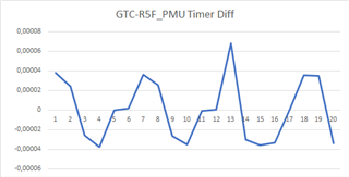
    It looks like that we have some oscillation between these two Timers.

    Could this effect to be caused due to the circumstance, that with the frequency of 22579200Hz the 2GHz
    target frequency could mathematically not really reached. There is still an error of 1Hz because of remainder.

    I had another question, how long does it take after activation of the HFOSC1 oscillator that this is in the steady-state?

    Kind Regards
    Thomas Willetal

  • Thomas,

    Certainly, I agree with your PLL calculations.
    When you read a system register, there is some latency -- I have seen at least 1us. You will need to factor that cross-device latency into your calculations for comparing PMU and GTC. I don't see how this comparison proves the clock is right since you are comparing two timers on the same timebase.

    I have recently run a test in which I compared the differences between a DMTIMER and the GTC; if you chose to do that, you should use a DMTIMER on the MCU side that will be operating from OSC0.

    Oscillator start-up time is difficult; it depends upon the board as well as the SoC. One way to determine that the oscillator is valid is to setup the DCC to HFOSC_1 and wait till you get a valid frequency.

    Kevin

  • Hi Kevin,

    thank your for your hints. We are using one of the R5F main domain cores for a realtime communication.
    To accomplish this task, the R5F PMU clock speed must be in sync with GTC clock speed.
    After the hfsoc1 switch over, it looks like there is any kind of oscillation between these timers.

    1. Do you have any further idea, what could be the reason?
    2. Could be error of 1Hz responsible for such behavior, caused by generating of the 2GHz from 22579200Hz clock source?
    3. Is it possible, that the sciserver is resetting the PLL clock adjustments later again?
    (because the PLL registers were initialized by the sciclient-direct and afterwards modified for the required PLL values)

    Kind Regards
    Thomas

  • Thomas,

    "My test is:
    "- Run a cyclic Task on a R5F Main domain with a cycle rate of 1s.
    "- Get value of the GTC,with HFSOC1 switch, and the PMU Timer, running at R5F with HFSOC1 switch.
    "- Compare these to timers if these are running with the same speed."

    -1-

    GTC can be clocked by:
    0010 8030h CTRL_MMR_CFG0_GTC_CLKSEL

    4'b0000-MAIN_PLL3_HSDIV1_CLKOUT
    4'b0001-MAIN_PLL0_HSDIV6_CLKOUT
    4'b0010-MCU_CPTS_REF_CLK (pin)
    4'b0011-CPTS_RFT_CLK (pin)
    4'b0100-MCU_EXT_REFCLK0 (pin)
    4'b0101-EXT_REFCLK1 (pin)
    4'b0110-SERDES0_IP2_LN0_TXMCLK
    4'b0111-SERDES0_IP2_LN1_TXMCLK
    4'b1000-SERDES0_IP2_LN2_TXMCLK
    4'b1001-SERDES0_IP2_LN3_TXMCLK
    4'b1010-SERDES1_IP2_LN0_TXMCLK
    4'b1011-SERDES1_IP2_LN1_TXMCLK
    4'b1100-SERDES0_IP1_LN2_TXMCLK
    4'b1101-SERDES1_IP3_LN2_TXMCLK
    4'b1110-MCU_PLL2_HSDIV1_CLKOUT
    4'b1111-MAIN_SYSCLK0

    Can you read this register?

    -2-

    I assume that you are running the Main R5F core from the PLL with OSC1. Can you confirm? 

    -3- 

    Suppose that the GTC and PMU are running at the same frequency. The details of the PLL do not come into play, here.

    Kevin

  • Hi Kevin,

    the GTC Timer is configured to run with the "MAIN_PLL0_HSDIV6_CLKOUT" frequency.

    jolly-joliot ~ # k3conf read 0x00108030
    |------------------------------------------------------------------------------|
    | VERSION INFO |
    |------------------------------------------------------------------------------|
    | K3CONF | (version 0.3-nogit built Thu Feb 29 11:51:13 UTC 2024) |
    | SoC | J784S4 SR1.0 |
    | SYSFW | ABI: 3.1 (firmware version 0x0009 '9.2.4--v09.02.04 (Kool Koala))') |
    |------------------------------------------------------------------------------|
    
    Value at addr 0x108030 = 0x1


    The value of the PLL0_HSDIV6_CTRL0 is 0x00008004 -> so a divider value of 5 is used.

    The GTC clock calculation is:

    HFOSC1 * (PLL0_FREQ_CTRL0 + PLL0_FREQ_CTRL1/2^24) = PLL0_FREQ
    22579200Hz * ( 0x58(88) + 0x0093bcaa(9682090)/2^24) = 2000000001Hz

    The PLL0_DIV_CTRL register is: 0x01020001 so a POST_DIVIDER of 2 is used.

    PLL0_FREQ / 2 = PLL0_OUT
    2000000001Hz / 2  = 1000000000Hz (I hope my assumption is correct, what happens with this skewed value ? )

    PLL0_OUT / MAIN_PLL0_HSDIV6_CLKOUT = GTC_CLKSEL
    1000000000Hz / 5 = 200000000Hz

    jolly-joliot ~ # k3conf dump clock 61
    |------------------------------------------------------------------------------|
    | VERSION INFO                                                                 |
    |------------------------------------------------------------------------------|
    | K3CONF | (version 0.3-nogit built Thu Feb 29 11:51:13 UTC 2024)              |
    | SoC    | J784S4 SR1.0                                                        |
    | SYSFW  | ABI: 3.1 (firmware version 0x0009 '9.2.4--v09.02.04 (Kool Koala))') |
    |------------------------------------------------------------------------------|
    
    |------------------------------------------------------------------------------------------------------------------------------|
    | Device ID | Clock ID | Clock Name                                                        | Status          | Clock Frequency |
    |------------------------------------------------------------------------------------------------------------------------------|
    |    61     |     0    | DEV_GTC0_GTC_CLK                                                  | CLK_STATE_READY | 200000000       |
    |    61     |     1    | DEV_GTC0_GTC_CLK_PARENT_HSDIV4_16FFT_MAIN_3_HSDIVOUT1_CLK         | CLK_STATE_READY | 250000000       |
    |    61     |     2    | DEV_GTC0_GTC_CLK_PARENT_POSTDIV3_16FFT_MAIN_0_HSDIVOUT6_CLK       | CLK_STATE_READY | 200000000       |
    |    61     |     3    | DEV_GTC0_GTC_CLK_PARENT_BOARD_0_MCU_CPTS0_RFT_CLK_OUT             | CLK_STATE_READY | 0               |
    |    61     |     4    | DEV_GTC0_GTC_CLK_PARENT_BOARD_0_CPTS0_RFT_CLK_OUT                 | CLK_STATE_READY | 0               |
    |    61     |     5    | DEV_GTC0_GTC_CLK_PARENT_BOARD_0_MCU_EXT_REFCLK0_OUT               | CLK_STATE_READY | 0               |
    |    61     |     6    | DEV_GTC0_GTC_CLK_PARENT_BOARD_0_EXT_REFCLK1_OUT                   | CLK_STATE_READY | 0               |
    |    61     |     7    | DEV_GTC0_GTC_CLK_PARENT_WIZ16B8M4CT3_MAIN_0_IP2_LN0_TXMCLK        | CLK_STATE_READY | 0               |
    |    61     |     8    | DEV_GTC0_GTC_CLK_PARENT_WIZ16B8M4CT3_MAIN_0_IP2_LN1_TXMCLK        | CLK_STATE_READY | 0               |
    |    61     |     9    | DEV_GTC0_GTC_CLK_PARENT_WIZ16B8M4CT3_MAIN_0_IP2_LN2_TXMCLK        | CLK_STATE_READY | 0               |
    |    61     |    10    | DEV_GTC0_GTC_CLK_PARENT_WIZ16B8M4CT3_MAIN_0_IP2_LN3_TXMCLK        | CLK_STATE_READY | 0               |
    |    61     |    11    | DEV_GTC0_GTC_CLK_PARENT_WIZ16B8M4CT3_MAIN_1_IP2_LN0_TXMCLK        | CLK_STATE_READY | 0               |
    |    61     |    12    | DEV_GTC0_GTC_CLK_PARENT_WIZ16B8M4CT3_MAIN_1_IP2_LN1_TXMCLK        | CLK_STATE_READY | 0               |
    |    61     |    13    | DEV_GTC0_GTC_CLK_PARENT_WIZ16B8M4CT3_MAIN_0_IP1_LN2_TXMCLK        | CLK_STATE_READY | 0               |
    |    61     |    14    | DEV_GTC0_GTC_CLK_PARENT_WIZ16B8M4CT3_MAIN_1_IP3_LN2_TXMCLK        | CLK_STATE_READY | 0               |
    |    61     |    15    | DEV_GTC0_GTC_CLK_PARENT_HSDIV4_16FFT_MCU_2_HSDIVOUT1_CLK          | CLK_STATE_READY | 200000000       |
    |    61     |    16    | DEV_GTC0_GTC_CLK_PARENT_K3_PLL_CTRL_WRAP_MAIN_0_CHIP_DIV1_CLK_CLK | CLK_STATE_READY | 500000000       |
    |    61     |    17    | DEV_GTC0_VBUSP_CLK                                                | CLK_STATE_READY | 125000000       |
    |------------------------------------------------------------------------------------------------------------------------------|

    ########
    The R5F PMU counter:


    The R5F MAIN is provided by the PLL14. This PLL has the same setttings as the PLL0 and used also the hfsoc1
    The R5F is running with 1GHz and so the PMU timer has a time base of 1ns.
    The GTC timer as time base of 5ns.

    To be able to compare the PMU timer with the GTC timer, the GTC counter value must be multiplied by a factor of 5.

    My fear is that the skewed value of 2000000001Hz triggered by a quartz with 22579200Hz is responsible for our problems, what do you think?

    Thank you for your assistance
    Kind Regards
    Thomas

  • Thomas,

    I have run code from R5F and monitor DMTIMER and GTC. I see a periodic waveform as well. I think this is because there is a latency across the chip and my read may step across the latency so that periodically, I have an extra latency in my measurement. To test this, I added a random delay which destroyed the periodicity.

    I do NOT think that the 0.67Hz offset is responsible for this. 

    It seems important to me that there is NO offset between the timers since both are clocked by the 200MHz + 1Hz clock (though divided differently).

    Kevin

  • Hello Kevin,

    Thank you for your support. I have modified the PLL settings to get 1Hz error reduced.
    I have set the PLL pre-divider to the oscillator input divider to the factor 2 and adjusted the GAIN of the PLL.

    OSC1 / PLL_REV_DIV = PLL_IN
    22579200Hz / 2 = 11289600Hz

    HFOSC1 * (PLL0_FREQ_CTRL0 + PLL0_FREQ_CTRL1/2^24) = PLL0_FREQ
    11289600Hz* ( 0xB1(177) + 0x277953(2586963)/2^24) = 2000000000Hz

    Would this to be OK? The behavior is a little bit better but not really OK.

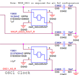
    I have another question. At our custom boards there are two different oscillators with different frequency fluctuation in ppm:

    HFSOC0: 19,2 MHZ with 10PPM -> +- 192Hz
    HFSOC1: 22,5792MHZ with 15PPM ->  +- 338.688 Hz

    Can the different oscillator accuracy be a problem?
    I have seen that the PLLs have a calibration feature, would that to be helpful?

    Kind Regards
    Thomas

  • Thomas,

    We continue to have a disconnect in this topic.

    I agree that the physically different oscillators on different board could create marginally different frequencies (e.g. 19.2MHz +/- 192 Hz). BUT, when you select PLL0, PLL8, PLL9, and PLL14 to all use the physically identical crystal, you have NO marginality to consider. What I mean is that you have defined:
    PLL0 = x/1*(88.577)
    PLL8 = x/1*(88.577)
    PLL9 = x/1*(88.577)
    PLL14= x/1*(88.577)

    So, I agree that if you modify x, you will get a varied frequency BUT all of these domains will see the same frequency. Therefore, counters run on these different clock domains should all see the same frequency.

    I would not divide the crystal by 2 and then multiply by 177... You will not get an exact 2GHz so you are not solving your perceived problem. As you read across the SoC, you will have read latencies that will account for some level of uncertainty in the counts.

    Calibration is, for this PLL, a jitter idea. It will not change your average frequency. It is most useful in a system where period jitter can be a problem (e.g. PCIe3 or something equivalent).

    Kevin

  • Hi Kevin,

    Many thanks, we currently have an interim solution in which the behavior is OK for us for the time being. I have two weeks holiday and then I would send you a minimal example of our application purpose. Would this Ok for you?

    Kind Regards
    Thomas