This thread has been locked.

If you have a related question, please click the "Ask a related question" button in the top right corner. The newly created question will be automatically linked to this question.

What powers the 5509A system clock PLL?

Other Parts Discussed in Thread: TPS62050

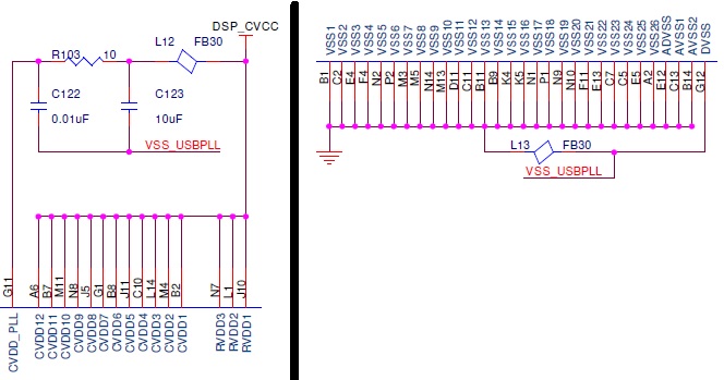
Perusing the 553x data sheet, I noticed that these devices have dedicated power and ground pins for the system clock PLL. That made me wonder: What power and ground pins are associated with the system clock PLL on the 5509A? Experience has shown that the PLL in this part is rather prone to losing lock, so it would be desirable to provide some extra filtering on its supply. Are there specific pins that power this? There's no mention in the data sheet.

David

  • David,

    C5509A and C5515 are 2 different design with different PLL module.

    Regards.

  • Understood, but my question still stands: What power rail is the 5509A PLL running off, and is there a particular pair of power/ground pins that are powering that particular subsystem?


  • Hi David,

    USBPLLVDD (G11) and USBPLLVSS (G12) are the dedicated supply and ground pins for the USB PLL, respectively. (Pin location shown for GHH and ZHH Packages)

    The USB module input clock is used by both the CPU PLL and the USB module PLL.

    USBPLLVDD is between 1.2V & 1.6V (depending on SYSCLK frequency required).

    Take a look at the DSK5509A schematics on Spectrum Digital's Support Page: http://c5000.spectrumdigital.com/dsk5509a/

    The PLL supply and GND use ferrite beads for noise suppression from the digital core voltage supplies and GNDs . See below...

    Hope this helps,
    Mark

  • Thanks for your reply, Mark, but I'm not actually using the USB PLL.  My question was about the PLL that generates the internal CPU clock. I run this at 144 MHz from a 12 MHz crystal. I am testing its performance by measuring McBSP and CLK_OUT pins which are divided versions of it. Using an Agilent 53230A counter (great tool, BTW) I am seeing what looks like occasional PLL cycle slipping. (Some 5509A chips seem to do it much more than others.) I'm trying to determine if there's anything I can do at the board level to improve this. I already have a Pi filter on the Vcore supply, which comes from a TPS62050 switcher. The 3.3V I/O supply comes from a linear regulator. The crystal signal itself looks good: nicely sinusoidal at ~3.3 Vpp, with 2nd and 3rd harmonics 20 dB down.

    David


  • Hi David,

    I'm pretty sure the System PLL and USB PLL use the same crystal on pins X1 and X2/CLKIN.

    How does the voltage look from the switcher, after the pi filter? Any ripple?

    USB PLL is susceptible to power supply ripple. The maximum allowable supply ripple is 1% for 1 Hz to 5 kHz; 1.5% for 5 kHz to 10 MHz; 3% for 10 MHz to 100 MHz, and less than 5% for 100 MHz or greater.

    I will check out the Agilent 53230A. Thanks for the tip.

    Regards,
    Mark

  • Hello Mark, I'm finally getting back to working on this issue.

    I hadn't done anything special with the USB PLL supply pin, because I'm not using the USB subsystem and the data sheet did not say that this pin also powers the main clock PLL.  My Vcore supply is generated by  a TPS62050 switchmode supply running at 600 kHz, so there is some ripple, but it's small enough that I had difficulty measuring it in the face of ground bounce from the DSP.

    I hacked up my circuit board to add a simple single-pole filter (1.5 kHz cutoff) on the USB PLL supply pin, and saw a statistically significant reduction in jitter spikes. The standard deviation of my clock frequency went down by a factor of two. This doesn't completely solve my problem, but it demonstrates that the approach is valid. Based on this experiment, I can justify spinning my circuit board.

    I'm thinking of adding a linear regulator specifically for the USB PLL supply pin. The complication is that my design changes the Vcore supply voltage dynamically with clock rate. Is it safe to use a fixed voltage for the USB PLL supply? I'm concerned that there might be some internal connection between the USB PLL supply and the other Vcore supply pins. Is it permitted to run the USB PLL a few tenths of a volt higher or lower than Vcore?

    Regards,

    David


  • Hi David,

    Thanks for your patience.

    Short answer - I'm not sure if you can supply different voltage for CVDD and USBPLLVDD so I have forwarded your question to someone who might know with certainty.

    Let us see what his response is.

    Best Regards,
    Mark

  • David,

    I found out the answer -  The USBPLLVDD pin should be powered with the same value as CVDD.

    I'm told there is no jitter issue with the C5509A DSK - http://c5000.spectrumdigital.com/dsk5509a/

    Do you already have this EVM to compare against your design?

    Best Regards,
    Mark