This thread has been locked.

If you have a related question, please click the "Ask a related question" button in the top right corner. The newly created question will be automatically linked to this question.

PROCESSOR-SDK-J784S4: Implementing PCIE driver for the R5F

Part Number: PROCESSOR-SDK-J784S4

Tool/software:

Hello,

I'm currently working on pcie support for the r5f of the j784s4 and I'm running into a problem when I try to put serdes into a reset state.

When I run the following code:

print("before by en\n");
CSL_FINSR(*(volatile uint32_t *)(uintptr_t)(baseAddr + 0x404),31,31, 0x1);
print("after en\n");

In trace0 of the remote core, I only have the message "before by en" printed.

The message "after by en" is missing, which indicates that the CSL_FINSR command is creating an unexpected interruption in the program's execution. Perhaps due to incorrect memory access.

We are assigning the value defined by CSL_WIZ16B8M4CT3_0_WIZ16B8M4CT3_BASE to the baseAddr of the command, because our objective is to use the pcie0 that is associated with serdes1 and the wiz1 mux.

However, we have already assigned the values ​​defined by CSL_WIZ16B8M4CT3_1_WIZ16B8M4CT3_BASE, CSL_WIZ16B8M4CT3_2_WIZ16B8M4CT3_BASE and CSL_WIZ16B8M4CT3_3_WIZ16B8M4CT3_BASE. And with all these values ​​we have the same behavior, an unexpected interruption of the program execution.

Apart from this, at DTS level, we have disabled the following nodes to avoid creating possible interference:
serdes0, serdes_wiz0, pcie0_rc, pcie0_ep, pcie1_rc, pcie1_ep.

Our setup: j784s4 as root complex connected to an am64x as endpoint (but the rules don't matter in the state I'm in)
Jacinto SDK: 09.01.00.22

Can you help, please? Any comments on this subject?

Best regards,
Joao Lima

  • Hi Joao,

    Again, I will need to preface my response with TI support will be limited for this topic. 

    As for comments, I used our Linux driver for reference, but I see that there is a wiz_clock_init function that is called before wiz_init:

    https://git.ti.com/cgit/ti-linux-kernel/ti-linux-kernel/tree/drivers/phy/ti/phy-j721e-wiz.c?h=ti-linux-6.1.y#n1593

    wiz_init calls wiz_reset, which writes to por_en bit at offset 0x404, so from this it looks like clock needs to be enabled before por_en is toggled. Can you confirm clock is set up for the WIZ wrapper before toggling en?

    Regards,

    Takuma

  • Hello Takuma,

    Thank you for your answer.

    The reference you shared was helpful in understanding potential issues, which led me to resolve the issue I was having.

    With the help of k3conf ( k3conf dump clock | grep PCIE0), I noticed that the clock associated with wiz0 was not ready. To fix this, I made sure in the dts file that the status of serdes0 and wiz0 are ok.

    After that, I ensured in the code that the base address is CSL_WIZ16B8M4CT3_0_WIZ16B8M4CT3_BASE and the device number is 1.

    To test, just start the board, create the link to the remote proc core and start the core state. The application with serdes initialization launched without any problems.
    Just for your information, rebooting does not start the application correctly. I have to repeat the steps I described previously. But, I will debug after the pcie driver is fully implemented and I will share the status about this. Meanwhile, I will update this thread with more questions.

    Thank you.

    References:
    3.2.2.17. SERDES — Processor SDK Linux for J784s4 Documentation

    Best regards,
    Joao Lima

  • Hi Joao,

    Glad I could help! 

    Regards,

    Takuma

  • Hello Takuma,

    Now I have a problem related to SRIS (Separate Reference Clock with Independent SSC) control.
    To make it easier to understand, I will share the function I currently have.

    void Pcie_srisControl (Pcie_Handle handle, uint32_t enable)
    {
        Pcie_DeviceCfgBaseAddr *cfg = Pcie_handleGetBases (handle);
    
        DebugP_assert(NULL != cfg);
    
        Pcie_DevParams *params = (Pcie_DevParams*)cfg->devParams;
    
        DebugP_assert(NULL != params);
        
        CSL_user_cfgRegs *userCfg = (CSL_user_cfgRegs *)params->userCfgBase;
    
        uint32_t val = userCfg->INITCFG;
    
        PCIE_SETBITS(val, CSL_USER_CFG_INITCFG_SRIS_ENABLE, enable);
    
        userCfg->INITCFG = val;
    }

    The code stops at execution of line 13, when I try to read the stored value from INITCFG. I've already tried reading the first parameters of the structure but the error persists.

    I have already confirmed with a print that the value of userCfgBase is 0x2917000UL, which is defined by the macro CSL_PCIE1_CORE_USER_CFG_USER_CFG_BASE in pdk_j784s4_09_01_00_22/packages/ti/csl/soc/j784s4/src/cslr_soc_baseaddress.h

    I am calling Pcie_srisControl after execute the serdesInit function correctly. This last is returning a successful status.

    Our intention is to use PCIe1.

    Any comments on this subject?

    Best regards,
    Joao Lima

  • Hi Joao,

    I can take a look at it tomorrow. But, as a shallow suggestion, is there a separate reference clock set up for SERDES (instead of the wiz wrapper around SERDES), or is there an external clock generator providing reference clock input to the SERDES module before interfacing with PCIe controller.

    Regards,

    Takuma

  • Hello Takuma,

    I will wait for more information about this.

    Thank you.

    Regards,
    Joao Lima

  • Hi Joao,

    In our Linux driver, the first access to user config register is within cdns_pcie_host_setup when this function calls cdns_pcie_start_link: https://git.ti.com/cgit/ti-linux-kernel/ti-linux-kernel/tree/drivers/pci/controller/cadence/pcie-cadence-host.c?h=ti-linux-6.1.y#n552

    And this cdns_pcie_host_setup is called from here: https://git.ti.com/cgit/ti-linux-kernel/ti-linux-kernel/tree/drivers/pci/controller/cadence/pci-j721e-host.c?h=ti-linux-6.1.y#n415

    Meaning, I see the following things that must happen before user config registers are registered:

    1. Initialize the phy: https://git.ti.com/cgit/ti-linux-kernel/ti-linux-kernel/tree/drivers/pci/controller/cadence/pci-j721e-host.c?h=ti-linux-6.1.y#n382 
    2. Initialize the PCIe reference clock: https://git.ti.com/cgit/ti-linux-kernel/ti-linux-kernel/tree/drivers/pci/controller/cadence/pci-j721e-host.c?h=ti-linux-6.1.y#n395 
    3. Wait for 100ms for reference clock to stabilize before deasserting PERST# signal to get PCIe out of reset: https://git.ti.com/cgit/ti-linux-kernel/ti-linux-kernel/tree/drivers/pci/controller/cadence/pci-j721e-host.c?h=ti-linux-6.1.y#n402 
    4. And finally enabling PTM responses here: https://git.ti.com/cgit/ti-linux-kernel/ti-linux-kernel/tree/drivers/pci/controller/cadence/pcie-cadence-host.c?h=ti-linux-6.1.y#n550

    Therefore, I would recommend checking through these steps once more to see that they are followed.

    Regards,

    Takuma

  • Hello Takuma,

    I hope you are well.

    In the meantime I was analyzing the J784S4's TRM document (SPRUJ52C – JUNE 2022 – REVISED JULY 2023) and the driver you suggested.
    Based on the documentation, we configured the ref clock to guarantee access to the user configuration (+information seen in Figure 12-119. PCIe subsystem block diagram).
    This analysis resulted in the following configuration to select core_refclk for torrent select MAIN_PLL2_HSDIV4_CLKOUT for 100 MHz in function CSL_serdesRefclkSel (location:ti-j784s4/pdk_j784s4_09_01_00_22/packages/ti/csl/src/ip/serdes_cd/V3/csl_serdes3.c). Within the functions used in this file, I confirmed the writing of the values ​​by reading them, to guarantee the correct W/R operations.

    With that in mind, can you confirm that the ref clock configuration is correct for configuring the serdes0 pcie1?
    github.com/.../pcie_serdes.c
    I would like to take this opportunity to ask the same thing about the line:
    github.com/.../pcie_soc.c

    I remember that the line where the program interrupts is:
    github.com/.../pcie_soc.c


    Any comments about this?

    Regards,
    Joao Lima

  • Hi Joao,

    Yes, MAIN_PLL2_HSDIV4_CLKOUT should be correct. From this, I assume you do not have an external clock generator to provide 100MHz, so you will need to enable ACSPCIe buffer to output PCIe refclk to connector like in this function: https://git.ti.com/cgit/ti-linux-kernel/ti-linux-kernel/tree/drivers/pci/controller/cadence/pci-j721e-host.c?h=ti-linux-6.1.y#n242

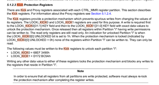
    Also, please check if CTRLMMR registers are actually being modified as these registers are protected by a LOCK_KICK register. Details in TRM:

    Regards,

    Takuma

  • Thank you Takuma,

    It's already solved. The offsets to write to the MMR registers were wrong. That's why the write operation to the blocks was always blocked.

    Thanks for the help.

    Regards,
    Joao Lima

  • Hello Takuma,

    I'm having an error when I try to read the contents of the status command register in the Pcie_readStatusCmdReg function, which in turn is called in the pcie_readregs function, and is in the pcie RC configuration function, as shown below:

    static int32_t Pcie_readStatusCmdReg(volatile const uint32_t *hwReg_STATUS_COMMAND_REGISTER, Pcie_StatusCmdReg *swReg)
    {
        int32_t status = SystemP_SUCCESS;
        uint32_t val;
    
        if ((hwReg_STATUS_COMMAND_REGISTER != NULL) && (swReg != NULL))
        {   
            DebugP_log("%s %d hwReg_STATUS_COMMAND_REGISTER = %p\n", __func__, __LINE__, hwReg_STATUS_COMMAND_REGISTER);
            val = swReg->raw = *hwReg_STATUS_COMMAND_REGISTER;
            DebugP_log("%s %d val = %d\n", __func__, __LINE__, val);
    
            ...
        }
    }
    
    int32_t Pcie_readRegs (Pcie_Handle handle, Pcie_Location location, Pcie_Registers *readRegs)
    {
      ...
    
      if ((status == SystemP_SUCCESS) && (readRegs->statusCmd != NULL))
      {
            status = Pcie_readStatusCmdReg (&(baseCfgEp->EP_PF_I_PCIE[params->pfNum].EP_PF_I_PCIE_BASE.I_COMMAND_STATUS), readRegs->statusCmd);
      }
      ...
    }
    
    int32_t Pcie_cfgRC (Pcie_Handle handle)
    {
        int32_t status = SystemP_SUCCESS;
    
        Pcie_Registers setRegs;
        Pcie_Registers getRegs;
        Pcie_StatusCmdReg statusCmd;
        Pcie_DevStatCtrlReg devStatCtrl;
        Pcie_AccrReg accr;
    
        status = Pcie_LtssmCtrl(handle, FALSE);
    
        memset (&setRegs, 0, sizeof(setRegs));
        memset (&getRegs, 0, sizeof(getRegs));
    
        getRegs.statusCmd = &statusCmd;
        status = Pcie_readRegs (handle, PCIE_LOCATION_LOCAL, &getRegs);
    
        ...
    }


    The code is being interrupted in the Pcie_readStatusCmdReg function on the 9 line.
    The print result of the previous line is:

    Pcie_readStatusCmdReg 1393 hwReg_STATUS_COMMAND_REGISTER = d800004


    On board's terminal, with devmem2, I can read the value stored at this address. The read register value is 0x100000. According to the excel registers of the j784s4, it is the expected value after the reset.

    we have already checked and tested unblocking different types of mmr domains. but we were unsuccessful.

    Do you have any comments that could help us unlock it please?

    Regards,
    Joao Lima

  • Hi Joao,

    Not sure if this will affect the issue, but looking through Linux driver, we enable PTM response before trying to start link (I assume starting link is what you are trying to achieve with the status command register):

    Otherwise, I would suggest checking the PCIe reference clock is toggling and PERST# signal is deasserted with a scope before trying to start the link.

    Regards,

    Takuma

  • Hello Takuma,

    Since the last message, I have taken a different approach to debugging the initialization of phy as a consequence of the pcie layer.

    Since our goal is to initialize the pcie driver in r5f, I started by studying all the configuration executed in the phy_j721e_wiz, phy_cadence_torrent, j721e-pcie drivers.

    This study resulted in a set of commands to configure the phy layer and the pcie layer. The initialization of wiz is done by the linux driver phy_j721e_wiz in the kernel space, leaving us only the responsibility of implementing the replication of the configuration of the phy_cadence_torrent and j721e-pcie drivers at the userspace level.

    You can find this replication implemented in a sh script in the following link:
    https://github.com/joaorl/ti-j784s4-pcie-r5f/blob/master/init/pcie_init.sh#L276

    As long as we can configure at the userspace level using the devmem2 tool, we can do the same at the r5f level.

    Looking at the script, I am having trouble getting the cmn_ready status, bit 0 of the wiz16b8m4ct3_PHY_PMA_CMN_REGISTERS_PHY_PMA_CMN_CTRL2__PHY_PMA_CMN_CTRL1 register (0x0506 E000h). This doesn't change status.

    Can you help me understand what might be missing to properly configure phy?

    drivers log file:
    ti-j784s4-pcie-r5f/init/log_wiz_phy_pci.txt at master · joaorl/ti-j784s4-pcie-r5f (github.com)

    Thank you.
    Joao Lima

  • Hi Joao,

    It looks like the only bit that is R/W is bit 5, which drives cmn_refclk_rcv_out_en. All other bits are reserved or read-only. 

    As for bit 0 status bit, this gets set once the SERDES goes out of reset. It should be the PHY_RESET_N field in SERDES_RST register, and phy_l{nnnn}_reset_n for reset of each link.

    Regards,

    Takuma

  • Hello Takuma,

    I reviewed the reset set and I already have the phy initialized. I say this because we get 0x0x00490011 when we read BASE_ADDRESS_PHY + 0xe000 and 0x0x00230000 when we read BASE_ADDRESS_PHY + 0xd014.

    (1) Is there another way to confirm that the PHY is initialized correctly?

    (2) Then we begin the pci block initialization process. However, we are unable to write to or read from pcie addresses such as BASE_ADDRESS_CFG=0x2917000 and BASE_ADDRESS_INTD=0x2910000. They always return a zero value.

    Another example is when I try to configure j721e_pcie_config_link_irq (BASE_ADDRESS_INTD + 0x108), the value 0x400 is not applied.

    (3) Another point is to enable Derived reference clock as default. what is the value of the address of the macro CMN_CDIAG_REFCLK_DRV0_CTRL_4

    https://git.ti.com/cgit/ti-linux-kernel/ti-linux-kernel/tree/drivers/phy/cadence/phy-cadence-torrent.c?h=ti-linux-6.1.y#%20n2080

    In the datasheet and in the excel file of the j784s4's registers, I didn't find anything related to the name and I can't find a connection point.

    (4) Do I have to do any extra configuration in wiz_clk_mux_set_parent, after initializing phy?

    Regards,
    Joao Lima

  • Hi Joao,

    Could you check registers 0x0506 040C, 0x0507 040C, 0x0502 040C, and 0x0505 040C?

    PCIe has a dependency on SERDES, so the reason why PCIe controller cannot be written could be that SERDES is not initialized. Otherwise, there are some CTRLMMR registers that need to be set for Endpoint vs Root Complex mode, link speed, and lane count, before PCIe controller is initialized.

    Regards,

    Takuma

  • Hello Takuma,

    The values ​​I am getting for 0x0506040C, 0x0507040C, 0x0502040C and 0x0505040C are:

    root@j784s4-evm:~# devmem2 0x0506040C
    Read at address 0x0506040C (0xffffb236340c): 0xA2800000
    
    root@j784s4-evm:~# devmem2 0x0507040C
    Read at address 0x0507040C (0xffff9154640c): 0x00000000
    
    root@j784s4-evm:~# devmem2 0x0502040C
    Read at address 0x0502040C (0xffffad56540c): 0xA2800000
    
    root@j784s4-evm:~# devmem2 0x0505040C
    Read at address 0x0505040C (0xffff9572c40c): 0x00000000

    I have already confirmed that the values ​​0x0507040C and 0x0505040C should be 0x22800000. I added the writing of these two registers to our script but I still can not write to the PCI registers.
    In the kernel driver logs it is not clear to me what else I should do to configure Serdes.

    After initializing the PHY, before the PCIe controller is initialized, I am writing to CTRL_MMR to configure the link speed, operation mode and count lane as follows:

    ++ j721e_pcie_set_link_speed ++
    [WRITE] addr: 0x104074 - curr value: 0x2 - expected value: 0x80
    Write to address 0x00104074 (0xffff9b3ed074): 0x00000080, readback 0x00000080
    
    ++j721e_pcie_set_mode++
    [WRITE] addr: 0x104074 - curr value: 0x80 - expected value: 0x82
    Write to address 0x00104074 (0xffffb63cb074): 0x00000082, readback 0x00000082
    
    ++j721e_pcie_set_lane_count++
    [WRITE] addr: 0x104074 - curr value: 0x82 - expected value: 0x182
    Write to address 0x00104074 (0xffffa040d074): 0x00000182, readback 0x00000182

    Regards,
    Joao Lima

  •  Hi Joao,

    For reference clock to SERDES (not PCIe), how is it being selected? Is TISCI API being used to select DEV_SERDES_10G0_CORE_REF_CLK parent clock to DEV_SERDES_10G0_CORE_REF_CLK_PARENT_HSDIV4_16FFT_MAIN_2_HSDIVOUT4_CLK (internal clock) or DEV_SERDES_10G0_CORE_REF_CLK_PARENT_BOARD_0_HFOSC1_CLK_OUT (external clock)? https://software-dl.ti.com/tisci/esd/latest/5_soc_doc/j784s4/clocks.html#clocks-for-serdes-10g0-device

    Also, for the reference clock coming from PCIe, is that using an external clock generator or using the SoC internal clock?

    Regards,

    Takuma

  • Hello Takuma,
    To ensure I am seeing the correct registers, can you provide the registers address to confirm, please?
    Meanwhile, for regs 0x00108400, 0x506 0408 and 0x506 040C, we got 0x00000003, 0x1810 0000 and 0xa280 0000.

    Consulting the k3conf, we got the following info for DEV_SERDES_10G0_CORE_REF_CLK_PARENT_HSDIV4_16FFT_MAIN_2_HSDIVOUT4_CLK :
    | 404 | 10 | DEV_SERDES_10G0_CORE_REF_CLK_PARENT_HSDIV4_16FFT_MAIN_2_HSDIVOUT4_CLK | CLK_STATE_READY | 100000000 |

    Regards,
    Joao

  • Hi Joao,

    The external vs internal clock depends on the board design if it is a custom board, or the PCIe slot if using the TI J784S4 EVM. For example, PCIe0 uses the external clock while the PCIe1 interface uses the internal clock on TI J784S4 EVM board.

    From EVM board, PCIe0 with external clock:

    , and PCIe1 with internal clock:

    When using internal SoC clock, then the following registers will need to be written to:

    https://e2e.ti.com/cfs-file/__key/communityserver-discussions-components-files/791/2084.enable_5F00_internal_5F00_ref_5F00_clock_5F00_out_5F00_pcie1_5F00_j784s4.patch

    Regards,

    Takuma

  • Hello Takuma,

    I added the code into the script I didn't resolve.

    In addition, running only the drivers and not the script, the results I get for the registers are:

    root@j784s4-evm:~# devmem2 0x108070
    /dev/mem opened.
    Memory mapped at address 0xffff99b90000.
    Read at address 0x00108070 (0xffff99b90070): 0x00000100
    root@j784s4-evm:~# devmem2 0x108074
    /dev/mem opened.
    Memory mapped at address 0xffffbae8c000.
    Read at address 0x00108074 (0xffffbae8c074): 0x00000100

    Values that are different that you are suggesting to write.

    Even so, I can do lspci to confirm the entry of pcie1 into the system, which may mean that the pcie was properly started by the driver.

    What else do you suggest?
    What is your availability to schedule a call?

    Regards,
    Joao 

  • Hi Joao,

    Again, TI support on this topic will be limited. The best we can offer are some suggestions. Otherwise, the recommendation is to use the Linux driver.

    As for suggestions, I tried adding some logs into the Linux driver to see which addresses are being read/written to and get the following:

    root@j784s4-evm:~# dmesg | grep DEBUG
    [ 5.659740] DEBUG: reading address 2910108
    [ 5.660813] DEBUG: writing address 2910108, with 2
    [ 5.660885] DEBUG: reading address 2910104
    [ 5.669934] DEBUG: writing address 2910104, with 400000
    [ 5.684010] DEBUG: reading address 2910104
    [ 5.689597] DEBUG: writing address 2910104, with c00000
    [ 5.700327] DEBUG: reading address 2910104
    [ 5.711069] DEBUG: writing address 2910104, with 1c00000
    [ 5.715493] DEBUG: reading address 2910104
    [ 5.720897] DEBUG: writing address 2910104, with 3c00000
    [ 5.737653] DEBUG: reading address 2917004
    [ 5.748675] DEBUG: writing address 2917004, with 1
    [ 5.754344] DEBUG: reading address 2917014
    [ 5.869847] DEBUG: reading address 2917014

    There looks to be some discrepancy with what is in TRM, but could you try doing something similar? You can also check these registers with devmem2, similar to what you did with the refclk registers.

    Regards,

    Takuma

  • Hello Takuma,

    Again, TI support on this topic will be limited.

    I understand that, but at this point, I am just asking how is the phy and the pcie block are initialized. I followed the driver, but there exist grey areas.
    Locking for the driver, I am not getting what are the Derived reference clock register. what is the value of the address of the macro CMN_CDIAG_REFCLK_DRV0_CTRL_4 (https://git.ti.com/cgit/ti-linux-kernel/ti-linux-kernel/tree/drivers/phy/cadence/phy-cadence-torrent.c?h=ti-linux-6.1.y#%20n2080)?

    Another question about the driver, what are the registers involved in the function wiz_clk_mux_set_parent. With the translations in the system I can't understand the base address.

    Can you help with these two questions?

    There looks to be some discrepancy with what is in TRM, but could you try doing something similar?

    As shared before (PROCESSOR-SDK-J784S4: Implementing PCIE driver for the R5F - Processors forum - Processors - TI E2E support forums),  I added some logs into the Linux driver to see which addresses are being read/written to and get the following. the log format consists of "[driver context][function name: line of code] message".

    Regards,
    Joao 

  • In pdk in the file pdk_j784s4_09_01_00_22/packages/ti/csl/src/ip/serdes_cd/V3/csl_serdes3.c, inside of the function CSL_serdesLaneEnable, on the following code snippet:

    /* Enable Refclk Out when the refclkout flag is set */
    if(serdesLaneEnableParams->refClkOut == CSL_SERDES_REFCLK_OUT_EN)
    {
    	if(serdesLaneEnableParams->refClkSrc == CSL_SERDES_REF_CLOCK_INT0 || serdesLaneEnableParams->refClkSrc == CSL_SERDES_REF_CLOCK_INT1)
    	{
    		/* 1. phy_en_refclk = 1'b0 (wiz) */
    		CSL_FINSR(*(volatile uint32_t *)(uintptr_t)(&torrent_sds_reg->WIZ_CONFIG.SERDES_RST),30,30,0x0);
    		CSL_FINSR(*(volatile uint32_t *)(uintptr_t)(&torrent_sds_reg->PHY_PCS_CMN_REGISTERS.PHY_ISO_CMN_CTRL),8,8,0x0);
    		/* 2. Write 0x0210 to CMN_CDIAG_REFCLK_DRV0_CTRL to select derived reference cock */
    		CSL_FINSR(*(volatile uint32_t *)(uintptr_t)(&torrent_sds_reg->PMA_CMN_REGISTERS.CMN_CDIAG_REFCLK_DRV0_CTRL),15,0,0x0210);
    		/* 3. Write 0x0118 to CMN_CDIAG_REFCLK_OVRD to enable derived reference clock */
    		CSL_FINSR(*(volatile uint32_t *)(uintptr_t)(&torrent_sds_reg->PMA_CMN_REGISTERS.CMN_CDIAG_REFCLK_TEST__CMN_CDIAG_REFCLK_OVRD),15,0,0x0118);
    		/* 4. Write 0x0401 to PHY_PIPE_CMN_CTRL1 to enable phy_en_refclk pin input */
    		CSL_FINSR(*(volatile uint32_t *)(uintptr_t)(&torrent_sds_reg->PHY_PCS_CMN_REGISTERS.PHY_PIPE_CMN_CTRL2__PHY_PIPE_CMN_CTRL1),15,0,0x0401);
    		/* 5. Set phy_en_refclk = 1'b1 */
    		CSL_FINSR(*(volatile uint32_t *)(uintptr_t)(&torrent_sds_reg->WIZ_CONFIG.SERDES_RST),30,30,0x1);
    		CSL_FINSR(*(volatile uint32_t *)(uintptr_t)(&torrent_sds_reg->PHY_PCS_CMN_REGISTERS.PHY_ISO_CMN_CTRL),8,8,0x1);
    	}
    }

    What are the address of the registers used on these two lines? are they 0x50600a0 and 0x5060098 or 0x5060050 and 0x506004c?:

    # /* 2. Write 0x0210 to CMN_CDIAG_REFCLK_DRV0_CTRL to select derived reference cock */
    	# CSL_FINSR(*(volatile uint32_t *)(uintptr_t)(&torrent_sds_reg->PMA_CMN_REGISTERS.CMN_CDIAG_REFCLK_DRV0_CTRL),15,0,0x0210);
    
    	# /* 3. Write 0x0118 to CMN_CDIAG_REFCLK_OVRD to enable derived reference clock */
    	# CSL_FINSR(*(volatile uint32_t *)(uintptr_t)(&torrent_sds_reg->PMA_CMN_REGISTERS.CMN_CDIAG_REFCLK_TEST__CMN_CDIAG_REFCLK_OVRD),15,0,0x0118);

    In the j784s4 registers map excel, I don't have any reference to this, only the pdk source code.

    Thanks.

    Regards,
    Joao

  • Hi Joao,

    It should be 0x0506 00a0 and 0x0506 0098.

    Likewise, I cannot find them for the J784s4 register map excel sheet. You may instead reference the J721E TRM for the register information (which is a bit harder to navigate). The registers should exist under J721E_registers4.pdf file in the zip file: https://www.ti.com/lit/zip/spruil1. J721E should also have the Torrent Serdes IP integrated, similar to J784s4, so the base physical address may be different, but offsets and register info should be the same.

    Regards.

    Takuma