This thread has been locked.

If you have a related question, please click the "Ask a related question" button in the top right corner. The newly created question will be automatically linked to this question.

TMS320C6748: Inquiries about the allocation of the TMS320C6748 chip Memory Map Summary

Part Number: TMS320C6748

Tool/software:

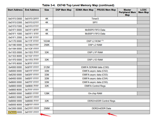
After reading Chapter 3.4 of the Memory Map Summary of the manual "TMS320C6748 Fixed- and Floating-Point DSP datasheet (Rev. G).pdf, there are some undefined memory, such as 0xD000 000 - 0xFFFF FFF, in fact, it is normal to read and write to the address behind the 0xD0000000 inside the program. I feel like it's working for 0xD0000000, and I'd like to confirm how this undefined memory segment is used.

  • Hello jehu liang

    Thank you for the query.

    Let me check internally with the expert and comeback.

    Regards,

    Sreenivasa

  • Hi Jehu

    Please see if the follow post helps you 

    https://e2e.ti.com/support/processors-group/processors/f/processors-forum/231157/omap-l138-internal-memory-ddr-data-space

     Original intent of the design was to be able to hook 512MB DDR2 memory but there were no such memories available in market that worked with the device family, so in order to ensure that customers do not assume incorrectly , we trimmed the memory map to show 256MB to ensure customers do not assume 512MB addressable memory even though that is the total addressable memory for external memory attach on this device 

    E000 8000 to FFFC FFFF is truly reserved  memory with nothing addressable on it etc. 

  • Hi  Mukul

              Thanks, I get it. Thank you very much for your answer.

  • Hi Mukul,

    I hope this message finds you well.

    Firstly, I would like to express my gratitude for your previous clarifications. Your insights were incredibly helpful.

    However, I have encountered an additional query that I believe requires your expertise.

    I am working with a core board featuring the TMS320C6748 processor, to which a 128MB DDR memory module is connected. According to my understanding, the theoretical addressing range for this DDR should span from 0xC0000000 to 0xC7FFFFFF. Yet, I've noticed that accessing the address 0xD0010000 within my program is possible without any issues, and both read and write operations are functioning as expected.

    This outcome has been quite puzzling to me. Under the condition where the TMS320C6748 is equipped with only a 128MB DDR, what device or memory region am I actually accessing when I attempt to access addresses beyond 0xD0000000?

    I am looking forward to your thoughts and guidance on this matter.

    Thank you very much for your time and assistance.

  • I will pass this to my colleague who is more knowledgeable in DDR design etc.

    Few questions 

    1) Are you sure there is no aliasing happening due to any data/address line swizzling

    2) Can you share more details of the DDR memory used and how it is connected to the the DSP 

    3) Is this a new design , how many boards exhibiting this 

  • Hi Mukul

    I would like to provide some additional context regarding the DDR memory addressing matter we've been discussing.

    This is not a new design but rather a core board that has already been in mass production. The core board is provided by Chuanglong, a supplier to our company. Jiehu Liang, an employee of Chuanglong, has confirmed that the DDR memory addressing range on this core board is indeed from 0xC0000000 to 0xC7FFFFFF.

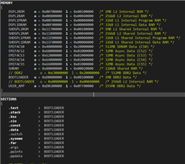
    Please find attached a diagram illustrating our bootloader program's address allocation scheme. All sections are designed to operate with run addresses following 0xD0000000. Each of our core boards is flashed with this specific bootloader program. We procure approximately 1000 units of this core board model annually, and to date, we have not encountered any issues. This indicates that each core board is able to access the memory range beyond 0xD0000000 without any problems.

    The development engineer responsible for the bootloader program has since left the company, and it was upon my review of the program that I noticed this discrepancy.

    In summary, we have a core board equipped with a 128M DDR peripheral, and the addressing range for this peripheral has been confirmed by the supplier to be from 0xC0000000 to 0xC7FFFFFF. Thousands of such core boards are able to access the memory range beyond 0xD0000000, yet at present, neither we nor the supplier have clarity on what device is being accessed in this range beyond 0xD0000000.

  • Hi Luo, this is most likely the result of address aliasing, where the upper address locations are actually accessing lower regions.

    To prove this, try writing to a location in the upper portion (eg 0xD0000000), and read at the same offset in the lower portion (eg, 0xC0000000).  If aliasing is occurring, you will see the same value in both locations, even though you only wrote to one of the addresses.  

    In other words, you should only be able to uniquely access 128MB (since that is the size of memory that you have), but the address range may seem larger because of aliasing.

    If your program expects to use both locations, then you will have a problem.  But based on you linker file, you are only allocating 0xD0000000-0xE0000000, so you won't see any issue.

    Regards,

    James

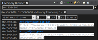
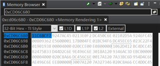
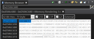
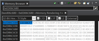
  • Hello James, thank you very much for your clarification. Following your guidance, I conducted an experiment, the details of which are shown in the figure. The conclusion is that all high address ranges can be mapped to 0xC000 0000 to 0xC7FF FFFF. The core board used for the experiment is equipped with a 128M DDR2, with a PageSize of 1024, a total of 8 banks, and a RowSize of 16384. Therefore, this DDR2 can only receive an addressing range of 128M. The phenomenon observed in the experiment is likely not caused by the DDR2 installed, but is probably due to the DSP. The logical addresses from 0xC000 0000 to 0xFFFF FFFF can all be accessed to the DDR.

  • thanks for the confirmation, will close this thread

    regards,

    James