This thread has been locked.

If you have a related question, please click the "Ask a related question" button in the top right corner. The newly created question will be automatically linked to this question.

[FAQ] AM620-Q1: Inputs required for DDR4 Signal Integrity Simulation

Part Number: AM620-Q1

Tool/software:

In one of our projects, we are using AM620-Q1_FCBGA441 where there is a necessity of DDR4 interface.

We need help from Texas side for the following details for signal integrity simulation:

1. on-die package decoupling parameters (C and R values).

2. recommended I/O drive strength for DQ,DQS,CLK and ADDRS nets for write and read cycles.

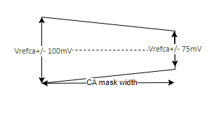
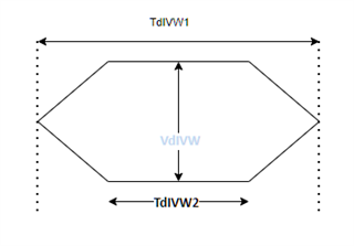
3. Targeted DDR4 eye mask definitions/requirements (CLK,ADDRS, DQ(read & write cycle), DQS(read & write cycle)). 

  • Hi All,

    Could you please help me with the above-mentioned queries?

    Regards,

    Asif P N

  • Hello - apologies for the delay with this response.

    1.
    Package RLC comes from AM62x AMC IBIS Model Component --> Package
    www.ti.com/.../sprm806

    On-die Decap
    Scale the on-die decap based on number of bits being simulated.
    You’ll use the full on-die decap value if you are simulating the whole interface (data and ACC) together.

    Example, for data byte0 we might set num_io = 11 to simulate 11 bits: DQ[7:0], DQSp/n, DM0. It would be more for address sim.

    **** DECAP ****
    .param  vddq_c = 6.985e-9

    .param  num_total_io    = 58
    .param  num_io                = 11

    Cvddq_c  DIE_VDDS_DDR             DIE_VDDS_DDR_c          vddq_c*num_io/num_total_io
    Rvddq_c  gnd                     DIE_VDDS_DDR_c          25.0036612e-3


    2.
    We recommend sweeping drive stregnth to identify those that give most margin.
    The idea however is to match impedance of the PCB trace typ
    - 40 ohm for Data
    - 40 or 60 for Address/Command

    3. JEDEC does not define eye masks for DDR4

    CA(Command/Address) Mask - DDR4 @ DRAM Die Pad 1600MT/s
    Shape    Trapezoid
    Height     Vrefca+/-100mV(setup),Vrefca+/-75mV(hold)
    Width     366ps + SR Derating (0.29280 tCK for 0 derating)

    Write Mask - DDR4 @ DRAM Die Pad 1600MT/s
    Shape    Rectangle
    Height     136mV
    Width    180.2ps (0.28832 UI)


    Read Mask - DDR4 @ SOC Die Pad 1600MT/s
    Shape    Hexagonal
    Height    VdIVW 136mV
    Width    
            TdIVW1 323.6ps (0.51776UI)
            TdIVW2 187.6ps (0.30016UI)

    Regards,
    Mark

  • Hi Mark,

    Thanks for your detailed inputs.

    Regards,

    Asif P N