Tool/software:
I have a few questions about layout design of LPDDR4 RAM which is used at the J784S4X eval board(E4-4.6).
I made comparison of layout design of LPDDR4 RAM and instructions which are given at the Jacinto 7 LPDDR4 Board Design and Layout Guidelines application note file.
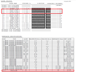
Questions are based on data group routing, CK and ADDR_CTRL routing specifications.
We are about the complete layout of our PCB, can you give us fast feedback?
- What kind of system level requirement should be defined to have less DQS propagation delay than CK pair? What kind of memory package calculations are done for this requirement? Can you give us an example?
DDR0_DQS0 and DDR0_DQS2 differential lines are longer than the CK pair for the U54 component at the eval board layout design. But, they should be shorter than the CK pair according to following requirement.

2. Why propagation delay of each DQS pair must be less than propagation delay of DQ/DM?
When I checkout the length of DQS pairs for U54 component at the eval board, I observe that each DQS pair almost have the same length with corresponding BYTEx at the layout of J784S4X eval board.
In other words, propagation delay of DQS pairs is not shorter than DQ/DM lines.

3. I have a question about length match of the ADDR_CTRL lines for the U54 component at the layout of J784S4X eval board. Why length match of DDR0_CA and DDR0_CKE lines is about 30 mil? I think it already exceeds 3ps skew time?,
I think that length of DDR0_CKE lines also should be 1330 mil.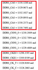
4. When I checked out the routing of DDR0_CK_C and DDR0_CK_T differential pair, they are also T-branch lines. At the T-branch point, routing is done with single ended impedance. According to PROC141E4_FAB document, single ended impedance value should be 66 ohm.
PCB designers of the eval board used 3 mils trace width to accomplish 66-ohm single ended impedance. When I checked out the trace impedance of this line by using a software tool, I realized that line impedance is not 66-ohm, it is about 55-ohm.
I think that this impedance mismatch is really important for the clock signals.
They can still reach out 4266 Mbit/s data rate in this case? Did they test the maximum data rate of the RAM on the eval board?