

Hi,
I would like to ask a question on EVMAM1808 board component footprints.
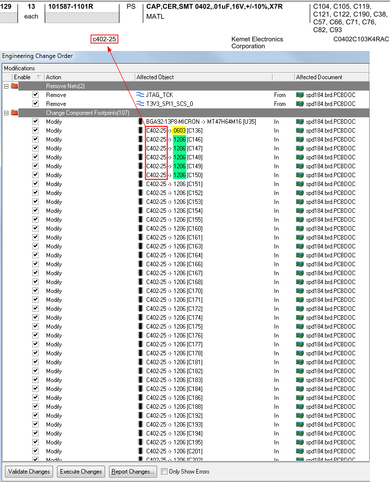
In EVMAM1808 board BOM, I see lots of footprint sizes like "C402-25", which are not EIA standards.
In addition, heading entries of Google search of "c402-25" are within SpectrumDigital site. There are only a very limited number of results from other sites, and from this it seems clearly that "c402-25" or alike {r402-25} are not industry standards, but are instead SpectrumDigital's internal naming conventions.
Besides the above, there are also inconsistencies between the schematic and PCB layout. As shown in the screenshot attached:
|
|
footprint in PCB |
footprint in schematic |
|
C136 |
C402-25 |
0603 |
|
C146 |
C402-25 |
1206 |
Of course, the actual footprint used on PCB should be the standard since the final board is accordingly manufactured. Then this indicates that the footprints specified in schematics are already out of date.
And what is the correspondence between you SpectrumDigital's convention {c402-25, r402-25} and industry standard such as EIA?
Zheng

